This thread has been locked.

If you have a related question, please click the "Ask a related question" button in the top right corner. The newly created question will be automatically linked to this question.

LAUNCHXL-F280049C: Converting 16 bit SPI communication code to 24 bits

Part Number: LAUNCHXL-F280049C
Other Parts Discussed in Thread: C2000WARE, DRV8311, DRV8376, DRV8316

Tool/software:

Hello,

I've been working on this for sometime and I'm really stuck so any help would be appreciated!

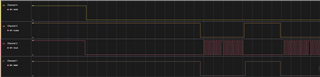
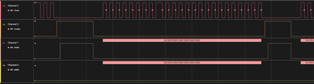
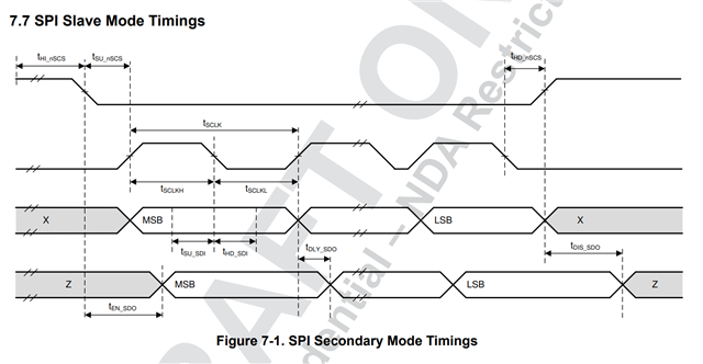
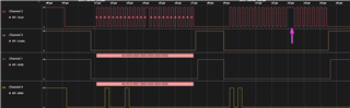
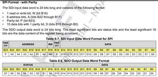
I have code that can communicate with a DRV device with a SPI frame of 16 bits, I'm trying to change this code so that I can communicate with another DRV device that has a SPI frame of 24 bits.

Here is the current code I have followed by the SPI frame I am trying to convert to:

void Config_evm_spi(void)
{
    //Pin Config
    EALLOW;
    // SPI_MOSI
    GPIO_SetupPinOptions(16, GPIO_INPUT, GPIO_ASYNC | GPIO_PULLUP);
    // SPI_MISO
    GPIO_SetupPinOptions(17, GPIO_INPUT, GPIO_ASYNC | GPIO_PULLUP);
    // SPI_CS
    GPIO_SetupPinOptions(56, GPIO_INPUT, GPIO_ASYNC | GPIO_PULLUP);
    // SPI_CLK
    GPIO_SetupPinOptions(57, GPIO_INPUT, GPIO_ASYNC | GPIO_PULLUP);

    GPIO_SetupPinMux(16, GPIO_MUX_CPU1, 1);
    GPIO_SetupPinMux(17, GPIO_MUX_CPU1, 1);
    GPIO_SetupPinMux(56, GPIO_MUX_CPU1, 1);
    GPIO_SetupPinMux(57, GPIO_MUX_CPU1, 1);
    EDIS;

    EALLOW;
    ClkCfgRegs.LOSPCP.all = 0;
    EDIS;

    // Initialize SPI FIFO registers
    SpiaRegs.SPIFFTX.all=0xE040;
    SpiaRegs.SPIFFRX.all=0x2044;
    SpiaRegs.SPIFFCT.all=0x0;

    //SPI Settings
    SpiaRegs.SPICCR.bit.SPISWRESET = 0;     //SPI Reset On
    SpiaRegs.SPICCR.bit.CLKPOLARITY = 0;    //SCLK Active High
    SpiaRegs.SPICCR.bit.SPICHAR = 0xF;      //16-bit SPI char
    SpiaRegs.SPICCR.bit.SPILBK = 0;

    SpiaRegs.SPICTL.bit.OVERRUNINTENA = 0;  //No overrun interrupt
    SpiaRegs.SPICTL.bit.CLK_PHASE = 0;      //Phase 0
    SpiaRegs.SPICTL.bit.MASTER_SLAVE = 1;   //Master mode
    SpiaRegs.SPICTL.bit.TALK = 1;           //nSCS enabled
    SpiaRegs.SPICTL.bit.SPIINTENA = 0;      //TX/RX Interrupt Disabled

    SpiaRegs.SPIBRR.bit.SPI_BIT_RATE = ((25000000 / 1000000) - 1);              //Set baud rate to 1MHz
    SpiaRegs.SPIPRI.bit.FREE = 1;           //Set so breakpoints don't disturb transmission
    SpiaRegs.SPICCR.bit.SPISWRESET = 1;   //Exit SPI reset

}

Uint16 spi_xmit(Uint16 spiFrame)
{
    SpiaRegs.SPITXBUF=spiFrame;

    //Wait for RX flag to indicate SPI frame completion
    while(SpiaRegs.SPIFFRX.bit.RXFFST != 1)
    {
    }

    return SpiaRegs.SPIRXBUF;
}

Uint16 spi_read(Uint16 addr)
{
    Uint16 commandword = 0;
    uint16_t p_addr = addr;
    uint16_t p_data = 0;

    uint16_t calc = ((p_addr << 9) & 0x7E00) | (p_data & 0x00FF);
    uint16_t parity = 0;
    while(calc)
    {
       parity ^= (calc & 1);
       calc >>= 1;
    }

    commandword = (0x8000 | (addr << 9) | (parity << 8));
    return spi_xmit(commandword);
}

Uint16 spi_write(Uint16 addr, Uint16 data)
{
    Uint16 commandword = 0;
    uint16_t p_addr = addr;
    uint16_t p_data = data;

    uint16_t calc = ((p_addr << 9) & 0x7E00) | (p_data & 0x00FF);
    uint16_t parity = 0;
    while(calc)
    {
       parity ^= (calc & 1);
       calc >>= 1;
    }

    commandword = ((addr << 9) | (parity << 8) | data);
    return spi_xmit(commandword);
}

I'm mostly concerned about the spi_read function for the time being, I feel like if I can get that to work I'd be able to figure out spi_write

Here is my attempt that's not working :

void Config_evm_spi(void)
{
//Pin Config
EALLOW;
// SPI_MOSI
GPIO_SetupPinOptions(16, GPIO_INPUT, GPIO_ASYNC | GPIO_PULLUP);
// SPI_MISO
GPIO_SetupPinOptions(17, GPIO_INPUT, GPIO_ASYNC | GPIO_PULLUP);
// SPI_CS
GPIO_SetupPinOptions(56, GPIO_INPUT, GPIO_ASYNC | GPIO_PULLUP);
// SPI_CLK
GPIO_SetupPinOptions(57, GPIO_INPUT, GPIO_ASYNC | GPIO_PULLUP);
GPIO_SetupPinMux(16, GPIO_MUX_CPU1, 1);
GPIO_SetupPinMux(17, GPIO_MUX_CPU1, 1);
GPIO_SetupPinMux(56, GPIO_MUX_CPU1, 1);
GPIO_SetupPinMux(57, GPIO_MUX_CPU1, 1);
EDIS;

EALLOW;
ClkCfgRegs.LOSPCP.all = 0;
EDIS;

// Initialize SPI FIFO registers
SpiaRegs.SPIFFTX.all = 0xE040;
SpiaRegs.SPIFFRX.all = 0x2044;
SpiaRegs.SPIFFCT.all = 0x0;

//SPI Settings
SpiaRegs.SPICCR.bit.SPISWRESET = 0;     //SPI Reset On
SpiaRegs.SPICCR.bit.CLKPOLARITY = 0;    //SCLK Active High
SpiaRegs.SPICCR.bit.SPICHAR = 0xF;      //16-bit SPI char
SpiaRegs.SPICCR.bit.SPILBK = 0;

SpiaRegs.SPICTL.bit.OVERRUNINTENA = 0;  //No overrun interrupt
SpiaRegs.SPICTL.bit.CLK_PHASE = 0;      //Phase 0
SpiaRegs.SPICTL.bit.MASTER_SLAVE = 1;   //Master mode
SpiaRegs.SPICTL.bit.TALK = 1;           //nSCS enabled
SpiaRegs.SPICTL.bit.SPIINTENA = 0;      //TX/RX Interrupt Disabled

SpiaRegs.SPIBRR.bit.SPI_BIT_RATE = ((25000000 / 1000000) - 1);              //Set baud rate to 1MHz
SpiaRegs.SPIPRI.bit.FREE = 1;           //Set so breakpoints don't disturb transmission
SpiaRegs.SPICCR.bit.SPISWRESET = 1;   //Exit SPI reset

}
Uint32 tspi_xmit(Uint32 spiFrame)
{
SpiaRegs.SPITXBUF = spiFrame;
//Wait for RX flag to indicate SPI frame completion
while(SpiaRegs.SPIFFRX.bit.RXFFST != 1)
{
}

return SpiaRegs.SPIRXBUF;

}
Uint32 tspi_read(Uint16 id, Uint16 addr)
{
Uint32 commandword = 0;
Uint16 data = 0; // No data to read
Uint16 p_addr = addr & 0x3F; // Ensure address is 6 bits (0-63)
// Construct the command word
commandword = (data & 0x7FFF) | (1 << 16) | (p_addr << 17); // 1 for read

// Calculate even parity for bits 0-15 and bits 16-23
Uint16 parity0 = 0, parity1 = 0;

int i;
for (i = 0; i < 16; i++) {
    parity0 ^= (commandword >> i) & 1;
}
for (i = 16; i < 24; i++) {
    parity1 ^= (commandword >> i) & 1;
}

// Set the parity bits
commandword |= (parity0 << 15) | (parity1 << 23);

return tspi_xmit(commandword);

}
Uint32 tspi_write(Uint16 id, Uint16 addr, Uint16 data)
{
Uint32 commandword = 0;
Uint16 p_addr = addr & 0x3F; // Ensure address is 6 bits (0-63)
// Construct the command word
commandword = (data & 0x7FFF) | (0 << 16) | (p_addr << 17); // 0 for write

// Calculate even parity for bits 0-15 and bits 16-23
Uint16 parity0 = 0, parity1 = 0;
int i;
for (i = 0; i < 16; i++) {
    parity0 ^= (commandword >> i) & 1;
}
for (i = 16; i < 24; i++) {
    parity1 ^= (commandword >> i) & 1;
}

// Set the parity bits
commandword |= (parity0 << 15) | (parity1 << 23);

return tspi_xmit(commandword);

}

Thank you!

Yara

  • Hi Yara,

    To clarify, our F28004x SPI module is capable of data word lengths from 1 to 16 data bits. We do not support 24 bit transactions inherently. Could you explain at a higher level how you are trying to send and receive the 24-bit data? How are you planning on breaking up break up the 24-bit data, since it will take more than one transaction? Since it will be two transactions, I imagine you should also be sending them back-to-back to ensure the chipselect remains low during the complete duration. Does you code run at the moment? Are you seeing specific errors? Sorry for all the questions- just wanting to get an understanding of the goal here and the specific trouble spot you are having.

    Also, have you already referred to our SPI examples in C2000Ware? ([C2000Ware]\driverlib\f28004x\examples\spi)

    Best Regards,

    Allison

  • Hi Allison,

    Thank you for confirming F28004x SPI module is only capable of 16 bit transactions, at the start I think I was running into this issue and only suspected this was the case. 

    As to how I would want to send a receive the 24 bit data, I think the easiest would be to handle the left most 8 bits followed by the right most 16 bits.

    I also have some code from one of our devices that has a 32 bit SPI frame if that would help? I believe its handled by sending 16 bits back to back.

    
    Uint16 tspi_read(Uint16 id, Uint16 addr8)
    {
        Uint16 p_addr;
        Uint16 p_data;
        Uint16 left8;
        Uint16 right16;
    
        Uint16 addr6 = addr8 & 0x3F;
    
        Uint16 dummy = 0;
    
        p_addr = spi_parity_calc(addr6);
    
        left8 = (p_addr << 15) | (addr6 << 9) | (id << 8);
        SpiaRegs.SPITXBUF=left8;
    
    
        p_data = 0;
    
        right16 = 0x00;
        SpiaRegs.SPITXBUF= right16;
        while(SpiaRegs.SPIFFRX.bit.RXFFST != 2);
    
    
        //return SpiaRegs.SPIRXBUF;
        return spi_xmit((left8 << 15) | (right16));
    }
    
    Uint16 tspi_write(Uint16 id, Uint16 addr, Uint16 data)
    {
    
        Uint16 p_addr;
        Uint16 p_data;
        Uint16 commandword;
        Uint16 dummy;
    
        //16-bit header
        p_addr = spi_parity_calc(addr);
        commandword = (id << 11) | (addr << 3) | (p_addr << 0);
        SpiaRegs.SPITXBUF=commandword; //transmit header
        dummy = SpiaRegs.SPIRXBUF;
    
        //16 bit data
        p_data = spi_parity_calc(data);
        commandword = p_data | data;
        SpiaRegs.SPITXBUF=commandword; //transmit data
    
        while(SpiaRegs.SPIFFRX.bit.RXFFST != 2); //wait for 2 words to receive in FIFO
    
        return SpiaRegs.SPIRXBUF; //return last word
    }

    My current code runs right now but the SPI communication to the device is all gibberish

    Thanks

    Yara

  • Hi Yara, 

    Running code is a good start so far- in spite of gibberish! We know the GPIO setup and connections are established. 

    I assume the chip select needs to remain low during the entire 24 or 32-bit transaction, so you should be sure to have F28004x send two back-to-back transmissions to send the upper and lower bits, and then reconstruct the data on the receiving end. What what is the other device part number? Have you verified that the data format, clock mode, chip select timing, etc. are all being met? This can corrupt data transactions if the devices don't agree.

    You can also use internal loopback mode (where TX and RX are tied together internally in F28004x) to check your SPI is successfully operating independent of the DRV device. 

    Best Regards,

    Allison

  • Hi Allsion,

    Chip select does need to remain low during the 24 bit transaction.

    so you should be sure to have F28004x send two back-to-back transmissions to send the upper and lower bits, and then reconstruct the data on the receiving end.

    I think this is where I'm really getting stuck and not sure how to do this correctly.

    What what is the other device part number? Have you verified that the data format, clock mode, chip select timing, etc. are all being met? This can corrupt data transactions if the devices don't agree.

    The other part that uses 32 bit SPI communication is the DRV8311, its SPI timing requirements are essentially the same as the one I'm working on, DRV8376 24 bit SPI

    Here is what my code is looking like so far, I based this off the DRV8311 code instead of DRV8316 

    Uint32 tspi_read(Uint16 id, Uint16 addr)
    {
    Uint32 commandword = 0;
    Uint16 data = 0; // No data to read
    Uint16 p_addr = addr & 0x3F; // Ensure address is 6 bits (0-63)
    // Construct the command word
    commandword = (data & 0x7FFF) | (1 << 16) | (p_addr << 17); // 1 for read
    
    // Calculate even parity for bits 0-15 and bits 16-23
    Uint16 parity0 = 0, parity1 = 0;
    
    int i;
    for (i = 0; i < 16; i++) {
        parity0 ^= (commandword >> i) & 1;
    }
    for (i = 16; i < 24; i++) {
        parity1 ^= (commandword >> i) & 1;
    }
    
    // Set the parity bits
    commandword |= (parity0 << 15) | (parity1 << 23);
    
    return tspi_xmit(commandword);
    
    }
    Uint32 tspi_write(Uint16 id, Uint16 addr, Uint16 data)
    {
    Uint32 commandword = 0;
    Uint16 p_addr = addr & 0x3F; // Ensure address is 6 bits (0-63)
    // Construct the command word
    commandword = (data & 0x7FFF) | (0 << 16) | (p_addr << 17); // 0 for write
    
    // Calculate even parity for bits 0-15 and bits 16-23
    Uint16 parity0 = 0, parity1 = 0;
    int i;
    for (i = 0; i < 16; i++) {
        parity0 ^= (commandword >> i) & 1;
    }
    for (i = 16; i < 24; i++) {
        parity1 ^= (commandword >> i) & 1;
    }
    
    // Set the parity bits
    commandword |= (parity0 << 15) | (parity1 << 23);
    
    return tspi_xmit(commandword);
    
    }

    and here is what the SPI transactions are looking like

    I'm not really sure where to proceed from here, looks like only 16 bit transactions are happening at a time.

    Thanks!

    Yara

  • Hi Allison,

    Just adding on here.

    I ran the DRV8311 code and I feel like I'm getting better results then the adjusted code

    Uint16 tspi_read(Uint16 id, Uint16 addr)
    {
        Uint16 p_addr;
        Uint16 p_data;
        Uint16 commandword;
    
        Uint16 dummy = 0xFF;
    
        p_addr = spi_parity_calc(addr);
        commandword = (0x8000) | (id << 11) | (addr << 3) | (p_addr << 0);
        SpiaRegs.SPITXBUF=commandword;
        dummy = SpiaRegs.SPIRXBUF;
    
        p_data = spi_parity_calc(dummy);
        commandword = (p_data << 15) | dummy;
        SpiaRegs.SPITXBUF=commandword;
        dummy = SpiaRegs.SPIRXBUF;
        while(SpiaRegs.SPIFFRX.bit.RXFFST != 2);
    
        dummy = SpiaRegs.SPIRXBUF;
        return SpiaRegs.SPIRXBUF;
    }
    
    Uint16 tspi_write(Uint16 id, Uint16 addr, Uint16 data)
    {
    
        Uint16 p_addr;
        Uint16 p_data;
        Uint16 commandword;
        Uint16 dummy;
    
        //16-bit header
        p_addr = spi_parity_calc(addr);
        commandword = (id << 11) | (addr << 3) | (p_addr << 0);
        SpiaRegs.SPITXBUF=commandword; //transmit header
        dummy = SpiaRegs.SPIRXBUF;
    
        //16 bit data
        p_data = spi_parity_calc(data);
        commandword = p_data | data;
        SpiaRegs.SPITXBUF=commandword; //transmit data
    
        while(SpiaRegs.SPIFFRX.bit.RXFFST != 2); //wait for 2 words to receive in FIFO
    
        return SpiaRegs.SPIRXBUF; //return last word
    }
    

  • Hi Yara,

    After you transmit, best practice is to check that there is valid complete data in the RXBUF before reading. Also, if you are always receiving 24-bit data, you could instead use 8-bit SPI character length. This way you can send 3 transmissions of 8-bits via TXFIFO and receive all three 8-bit character bits into RXFIFO. Are you using FIFO interrupts? You could just set the RXFFIL to 3, so that when you receive the three characters into the FIFO, the interrupt triggers and you can reconstruct the 24-bit data - here's the pseudocode:

    1. Transmit 3x8-bit data
      • Side note: the SPI FIFO is optimized for 16-bit data so when you transmit, the data you written to the TXBUF should be left justified, so you would bit-shift left << 8 before writing to TXBUF to transmit the desired data. This is not needed in the RXBUF since the device received data into the lower bits of the RXBUF - this is described in the TRM but thought I'd mention.
    2. Wait for RXFIFO level to show 3 RX FIFO levels are full with complete data.
      • This would trigger an RX interrupt if RXFFIL is set to 3 (when there are 3 or more words in the RXFIFO, interrupt is triggered)
    3. In the RX FIFO interrupt:
      • Read from the RXBUF 3 times to read the 3x8-bit data
      • When you read, you can save them each into 32-bit variables (since we don't have a 24-bit data type) and bit shift the data accordingly so that you can OR them to reconstruct the complete data. 

    You could adjust this if you want to use the 16-bit data - it would just be 2 transmissions (RXFFIL of 2) and you would have to adjust the shifting to extract the 16 bit data and 8 bit data. Are you already referring to any specific C2000ware example? We have some that implement FIFO interrupts you can refer to.

    Best Regards, 

    Allison

  • Okay I tired implementing your suggest, although I'm really not proficient in CCS and really just working with the examples I already have

    Are you already referring to any specific C2000ware example? We have some that implement FIFO interrupts you can refer to.

    I've been working with firmware that previous team members have written so they may have referenced C2000ware examples?

    This is what my code is looking like so far for my SPI read and write

    Uint32 tspi_read(Uint16 id, Uint16 addr)
    {
    Uint16 p_addr, p_data;
    Uint32 commandword;
    Uint16 dummy = 0xFF;
    Uint32 received_data = 0;
    Uint8 byte1, byte2, byte3;
    // Calculate parity for the address
    p_addr = spi_parity_calc(addr);
    
    // Construct 24-bit command word:
    // Bit 23: Parity bit for bits 16-23 (addr parity)
    // Bits 17-22: Address
    // Bit 16: Read (1)
    // Bits 0-14: Empty, set to 0
    Uint8 tx_byte1 = 0x00;
    Uint8 tx_byte2 = (1 << 7);
    Uint8 tx_byte3 = (p_addr << 7) | ((addr & 0x3F) << 1);
    
    // Transmit command word (send as 3x 8-bit)
    SpiaRegs.SPITXBUF = tx_byte1;  // First 8 bits
    SpiaRegs.SPITXBUF = tx_byte2;  // Middle 8 bits
    SpiaRegs.SPITXBUF = tx_byte3;  // Last 8 bits
    
    // Wait for RXFIFO to be full (3x 8-bit data)
    while (SpiaRegs.SPIFFRX.bit.RXFFST < 3);
    
    // Read the received data (3x 8-bit)
    byte1 = SpiaRegs.SPIRXBUF & 0xFF;
    byte2 = SpiaRegs.SPIRXBUF & 0xFF;
    byte3 = SpiaRegs.SPIRXBUF & 0xFF;
    
    received_data = ((Uint32)byte1 <<16) | ((Uint32)byte2 << 8) | ((Uint32)byte3);
    
    return received_data;
    }
    
    
    Uint32 tspi_write(Uint16 id, Uint16 addr, Uint16 data)
    {
    Uint16 p_addr, p_data;
    Uint32 commandword;
    Uint32 received_data = 0;
    Uint8 byte1, byte2, byte3;
    // Calculate parity for address and data
    p_addr = spi_parity_calc(addr);
    p_data = spi_parity_calc(data);
    
    // Construct 24-bit command word:
    // Bit 23: Parity bit for bits 16-23 (addr parity)
    // Bits 17-22: Address
    // Bit 16: Write (0)
    // Bits 0-15: Data with parity bit
    Uint8 tx_byte1 = (p_data << 7) | ((data >> 8) & 0x7F);
    Uint8 tx_byte2 = data & 0xFF;
    Uint8 tx_byte3 = (p_addr << 7) | ((addr & 0x3F) << 1);
    
    
    // Transmit command word (send as 3x 8-bit)
    SpiaRegs.SPITXBUF = tx_byte1;  // First 8 bits
    SpiaRegs.SPITXBUF = tx_byte2;  // Middle 8 bits
    SpiaRegs.SPITXBUF = tx_byte3;  // Last 8 bits
    
    // Wait for RXFIFO to be full (3x 8-bit data)
    while (SpiaRegs.SPIFFRX.bit.RXFFST < 3);
    
    // Read the received data (3x 8-bit)
    byte1 = SpiaRegs.SPIRXBUF & 0xFF;
    byte2 = SpiaRegs.SPIRXBUF & 0xFF;
    byte3 = SpiaRegs.SPIRXBUF & 0xFF;
    
    received_data = ((Uint32)byte1 <<16) | ((Uint32)byte2 << 8) | ((Uint32)byte3);
    
    return received_data;
    }

    I'm not really sure what is happening but it looks like two 24 bit transactions are happening when  ENABLE is low, so would be correct to conclude that I just need to figure out how to shorten the length of time ENABLE is low? Not really sure where or how to do this? 

    ...

    In the Configure_evm_spi function I see there is a line that mentions nSCS Enable

    Regards,

    Yara

  • Sorry for all the updates!

    I got 24 bit transactions so progress has somewhat been made!

    Uint32 tspi_read(Uint16 id, Uint16 addr)
    {
    Uint16 p_addr, p_data;
    Uint32 commandword;
    Uint16 dummy = 0xFF;
    Uint32 received_data = 0;
    Uint8 byte1, byte2, byte3;
    // Calculate parity for the address
    p_addr = spi_parity_calc(addr & 0x3F);
    
    // Construct 24-bit:
    // Bit 23: Parity bit for bits 16-23 (addr parity)
    // Bits 17-22: Address
    // Bit 16: Read (1)
    // Bits 0-14: Empty, set to 0
    Uint8 tx_byte1 = (p_addr << 7) | ((addr & 0x3F) << 1) | 1;
    Uint8 tx_byte2 = 0;
    Uint8 tx_byte3 = 0;
    
    // Transmit command word (send as 3x 8-bit)
    SpiaRegs.SPITXBUF = tx_byte1;  // First 8 bits
    SpiaRegs.SPITXBUF = tx_byte2;  // Middle 8 bits
    SpiaRegs.SPITXBUF = tx_byte3;  // Last 8 bits
    
    // Wait for RXFIFO to be full (3x 8-bit data)
    while (SpiaRegs.SPIFFRX.bit.RXFFST < 3);
    
    // Read the received data (3x 8-bit)
    byte1 = SpiaRegs.SPIRXBUF & 0xFF;
    byte2 = SpiaRegs.SPIRXBUF & 0xFF;
    byte3 = SpiaRegs.SPIRXBUF & 0xFF;
    
    received_data = ((Uint32)byte1 <<16) | ((Uint32)byte2 << 8) | ((Uint32)byte3);
    
    return received_data;
    }
    
    
    Uint32 tspi_write(Uint16 id, Uint16 addr, Uint16 data)
    {
    Uint16 p_addr, p_data;
    Uint32 commandword;
    Uint32 received_data = 0;
    Uint8 byte1, byte2, byte3;
    // Calculate parity for address and data
    p_addr = spi_parity_calc(addr);
    p_data = spi_parity_calc(data);
    
    // Construct 24-bit command word:
    // Bit 23: Parity bit for bits 16-23 (addr parity)
    // Bits 17-22: Address
    // Bit 16: Write (0)
    // Bits 0-15: Data with parity bit
    Uint8 tx_byte1 = (p_addr << 7) | ((addr & 0x3F) << 1) | 0;
    Uint8 tx_byte2 = ((p_data << 7) | ((data >> 8) & 0x7F));
    Uint8 tx_byte3 = data & 0xFF;
    
    
    // Transmit command word (send as 3x 8-bit)
    SpiaRegs.SPITXBUF = tx_byte1;  // First 8 bits
    SpiaRegs.SPITXBUF = tx_byte2;  // Middle 8 bits
    SpiaRegs.SPITXBUF = tx_byte3;  // Last 8 bits
    
    // Wait for RXFIFO to be full (3x 8-bit data)
    while (SpiaRegs.SPIFFRX.bit.RXFFST < 3);
    
    // Read the received data (3x 8-bit)
    byte1 = SpiaRegs.SPIRXBUF & 0xFF;
    byte2 = SpiaRegs.SPIRXBUF & 0xFF;
    byte3 = SpiaRegs.SPIRXBUF & 0xFF;
    
    received_data = ((Uint32)byte1 <<16) | ((Uint32)byte2 << 8) | ((Uint32)byte3);
    
    return received_data;
    }
    

    Now I'm running into the issue of the all the transactions essentially being 0s. I'm thinking this might be because it doesn't really look like the timing diagram:

    How would I be able to ensure that SD/ SDI wait a certain amount of time after nSCS goes low?

    Regards,

    Yara

  • Hi Yara,

    Good to see you are getting 24-bit transactions! If you are seeing zeros, it certainly could be a timing issue or perhaps a transmit/receive mechanism. Is the above snippet for the other (non-C2000) device? It looks like the clock line should be idle low, transmit data on the rising edge and receive/latch data on the falling edge which would be polarity = 0 and phase = 0 on the C2000. Assuming you have this already set, you should be ok on the clock mode. In the analyzer screenshot you posted above, it looks like the MISO and MOSI lines are sending zeros when chip select is low, though. Is this intentional?

    One way to isolate and test that the C2000 SPI module is working would be to enable internal loopback mode (this internally ties RX and TX together to loop back the SPI data). Can you try doing this and sending known data and check that you are receiving the same data back? This will help to understand if the SPI is set up correctly (can get more visibility into if you are sending correctly and receiving correctly by looking solely at the F28004x device).

    In regard to the chip select timings, this information is depending on the SPI speed and is detailed in our device datasheet:

    Best Regards,

    Allison

  • Hi Allison,

    Thank you so much for all your support!

    So I'm able to read all the registers without any issues, I'm close to getting my write function to work as well. I'm running into an issue though where some clock pulses are too long? to the point where a SPI transaction can happen because it throws off how many pulses there are.

    Why does this happen and how can I work around it?

    Also the thing that got my SPI transactions to really work is adding 0x0000 and shifting the needed bits further to the left. I'm glad it works but I don't really understand it?

    Regards,

    Yara

  • My logic analyzer sample rate was too low, first issue has been fixed! If you could just shed some insight on the second question that'd be great.

  • Hi Yara,

    This is great progress! Happy to see you have it working and figured out the sample rate question. In regards to your second question, is there a reason you are initializing tx_byte1 to 0x0000? tx_byte1 is declared as an 8-bit variable, but looks like you are shifting beyond the 8-bits so only the least significant 8 bits should be stored and this would likely result in cutting off the upper 8 bits of data.

    If you recall my earlier note, if you are transmitting 8-bit data, you should left-justify by bit-shifting left 8 before writing to TXBUF. Is that what is intended? Are you trying to write left-justified 16-bit data to the TXBUF to transmit? p_addr and addr_read are also 16-bit so that makes sense to me. My thought is perhaps before, you did not have the data properly left-justified.

    Best Regards,

    Allison