Because of the Thanksgiving holiday in the U.S., TI E2E™ design support forum responses may be delayed from November 25 through December 2. Thank you for your patience.

TMS320F28P550SJ: Use PGA as a buffer for ADC measurement

Part Number: TMS320F28P550SJ
Other Parts Discussed in Thread: SYSCONFIG

Tool/software:

Hi champs,

I am asking this for our customer.

The user wants to handle memory crosstalk issue and use the on-chip PGA as a buffer for ADC measurement.

For example,

Measure Signal with high source impedance.

Assume 56-pin QFN

Questions:

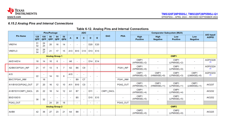
1. They only need to input Signal to Pin 7 (A2/B6/C9/PGA1_INP) of 56 QFN from PGA1_INP. Is it right?
2. Choose below mux (PMUX/NMUX/MMUX) as 0 for all.
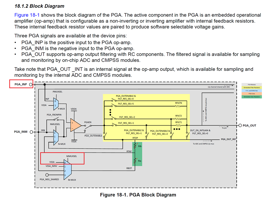
3. There are two - PGA_OUT and PGA_OUT _INT. They both can be used for ADC sampling. The difference is that PGA_OUT can be brought out to the pin, but PGA_OUT _INT cannot. Is our understanding correct?

4. In this case, the user does not want to bring PGA output to pin so they should use PGA_OUT _INT to A21/B21 (use PGA1_OUT_INT as an example). Is it right?

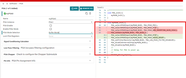
5. In Sysconfig,

How does the user change the ground pin to VSSA?

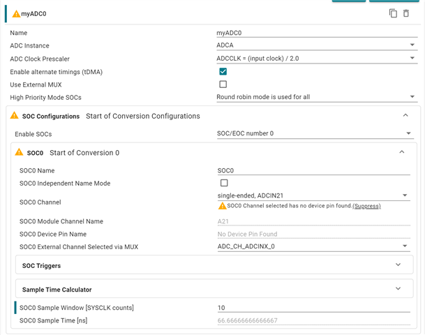
How does the user change the PGA1_OUT _INT to A21?

Would you please illustrate this in Sysconfig?

  • Hi Wayne,

    Here are answer to your questions:

    1) Yes, They only need to input Signal to PGA1_INP

    2) Yes, all muxes should be 0.

    3) Yes

    4) Yes

    5) A21 is not available for 56-pin package. let me ask other experts how to use buffor mode in this case.

    Regards,

    Hadi

  • Hi Hadi,

    What do you mean by "5) A21 is not available for 56-pin package. let me ask other experts how to use buffer mode in this case."?

    Isn't this an internal signal?

    But anyway, the user just want to use on-chip PGA as a buffer like what they do without an buffer.

    In other words, there is only one input signal pin and there is no other pin needed (neither another ground pin nor a PGA output).

  • Hi Hadi and/or champs,

    This is urgent.

    Do you have any update?

    Is there anything wrong with Sysconfig or the datasheet?

    For Q5 above,

    In Sysconfig,

    How does the user change the ground pin to VSSA?

    How does the user change the PGA1_OUT _INT to A21?

  • Hi Wayne,

    Apologies for the delay in response as Hadi is not out of office.

    The input (PGA_INP and PGA_INM) and output (PGA_OUT) in the Pin Info just shows the input and output pins are available at a specific pin. It is not a configurable option.

    For the buffer mode configuration, when we select the PGA Mode Selection as buffer mode, it will configure the MMUXSEL to VSSA.

    Regards,

    Meghavi

  • Hi Meghavi,

    How does the user use the PGA1_OUT _INT, A21 here?

    When the user chooses A21 after setting the PGA1 as buffer, it shows an error below.

    It shows there is no such pin.

    Is there anything wrong?

  • Hi Meghavi,

    Do you have any update?

    Would you please help confirm?

    1. We don't need to change anything about PGA1_OUT (A14/B14/C4/PGA1_OUT above) in Sysconfig even it is in grey. The user can use pin (A14/B14/C4/PGA1_OUT) like other ADC input pins for another purpose.

    2. We can use internal signal, PGA1_OUT_INT (A21) in the last post by suppressing it without any concern.