


Part Number: TMS320F280039C
Tool/software:
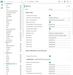
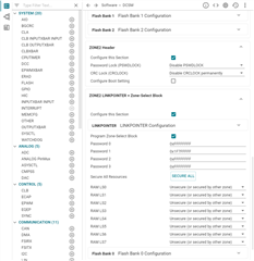
When I chang the configuration of DCSM to enable JTAGLOCK,the code not protected by ZONE.
The configuration of DCSM as follow:
I have got an error by using CCS to flash image (.out file) to MCU.
[ERROR] C28xx_CPU1: Error during Flash Programming. Address 0x00078028, FMSTAT (STATCMD on some devices) 0x00001010
This is first time to program OTP area.
;----------------------------------------------------------------------
; Zone 1
;----------------------------------------------------------------------
     .sect "dcsm_otp_z1_linkpointer"
      .retain
      .long 0x00003FFF
      .long 0x00003FFF
      .long 0x00003FFF

     .sect "dcsm_otp_z1_jlm_enable"
      .retain
      .long 0xFFFF0000     ;Z1OTP_JLM_ENABLE
     .sect "dcsm_otp_z1_jtag_pswdh"
      .retain
      .long 0x4BFFFFFE     ;Z1OTP_JTAGPSWDH0
      .long 0x3FFFFFFF     ;Z1OTP_JTAGPSWDH1

     .sect "dcsm_otp_z1_cmac_key"
      .retain
      .long 0x2B7E1516     ;Z1OTP_CMACKEY0
      .long 0x28AED2A6     ;Z1OTP_CMACKEY1
      .long 0xABF71588     ;Z1OTP_CMACKEY2
      .long 0x09CF4F3C     ;Z1OTP_CMACKEY3

     .sect "dcsm_otp_z1_pswdlock"
      .retain
      .long 0xFB7FFFFF

     .sect "dcsm_otp_z1_crclock"
      .retain
      .long 0x7FFFFFFF

     .sect "dcsm_otp_z1_gpreg"
      .retain
      .long 0x5AFFFFFF     ;Z1OTP_GPREG1 = Z1_BOOTPIN
      .long 0x5Affffff     ;Z1OTP_GPREG2
      .long 0xFFFFFF0A     ;Z1OTP_GPREG3 = Z1OTP_BOOTDEF_LOW
      .long 0xFFFFFFFF     ;Z1OTP_GPREG4 = Z1OTP_BOOTDEF_HIGH
     .sect "dcsm_zsel_z1"
      .retain
      .long 0xFFFFFF00     ;Z1OTP_CSMPSWD0 (LSW of 128-bit password)
      .long 0x4D7FFFFF     ;Z1OTP_CSMPSWD1
      .long 0xFFFFFFFF     ;Z1OTP_CSMPSWD2
      .long 0xFFFFFFFF     ;Z1OTP_CSMPSWD3 (MSW of 128-bit password)

      .long 0xAAAAAAAA     ;Z1OTP_GRABSECT1
      .long 0xAAAAAAAA     ;Z1OTP_GRABSECT2
      .long 0xAAAAAAAA     ;Z1OTP_GRABSECT3
      .long 0x0000AAAA     ;Z1OTP_GRABRAM1
      .long 0xFFFFFFFF     ;Reserved
      .long 0xFFFFFFFF     ;Reserved

      .long 0xFFFFFFFF     ;Z1OTP_EXEONLYSECT1
      .long 0x0000FFFF     ;Z1OTP_EXEONLYSECT2
      .long 0x000000FF     ;Z1OTP_EXEONLYRAM1
      .long 0xFFFFFFFF     ;Reserved
      .long 0xFFFFFFFE     ;Z1OTP_JTAGPSWDL0
      .long 0x2BFFFFFE     ;Z1OTP_JTAGPSWDL1


;----------------------------------------------------------------------

; For code security operation,after development has completed, prior to
; production, all other zone select block locations should be programmed
; to 0x0000 for maximum security.
; If the first zone select block at offset 0x10 is used, the section
; "dcsm_rsvd_z1" can be used to program these locations to 0x0000.
; This code is commented out for development.

;       .sect "dcsm_rsvd_z1"
;        .loop (1e0h)
;              .int 0x0000
;        .endloop


;----------------------------------------------------------------------
; Zone 2
;----------------------------------------------------------------------
     .sect "dcsm_otp_z2_linkpointer"
      .retain
      .long 0x00003FFF
      .long 0x00003FFF
      .long 0x00003FFF

     .sect "dcsm_rsvd_z2"
      .retain
      .long 0xFFFFFFFF     ;Reserved
     .sect "dcsm_otp_z2_pswdlock"
      .retain
      .long 0x1F7FFFFF

     .sect "dcsm_otp_z2_crclock"
      .retain
      .long 0x3FFFFFFF

;;     .sect "dcsm_otp_z2_gpreg"
;;      .retain
;;      .long 0x5AFFFFFF     ;Z2OTP_GPREG1 = Z2_BOOTPIN
;;      .long 0x5AFFFFff     ;Z2OTP_GPREG2
;;      .long 0xFFFFFFCA     ;Z2OTP_GPREG3 = Z2OTP_BOOTDEF_LOW
;;      .long 0xFFFFFFFF     ;Z2OTP_GPREG4 = Z2OTP_BOOTDEF_HIGH
     .sect "dcsm_rsvd1_z2"
      .retain
      .long 0xFFFFFFFF     ;Reserved
      .long 0xFFFFFFFF     ;Reserved

     .sect "dcsm_zsel_z2"
      .retain
      .long 0xFFFFFFFF     ;Z2OTP_CSMPSWD0 (LSW of 128-bit password)
      .long 0x1F7FFFFF     ;Z2OTP_CSMPSWD1
      .long 0xFFFFFFFF     ;Z2OTP_CSMPSWD2
      .long 0xFFFFFFFF     ;Z2OTP_CSMPSWD3 (MSW of 128-bit password)

      .long 0xAAAAAAAA     ;Z2OTP_GRABSECT1
      .long 0xAAAAAAAA     ;Z2OTP_GRABSECT2
      .long 0xAAAAAAAA     ;Z2OTP_GRABSECT3
      .long 0x0000AAAA     ;Z2OTP_GRABRAM1
      .long 0xFFFFFFFF     ;Reserved
      .long 0xFFFFFFFF     ;Reserved

      .long 0xFFFFFFFF     ;Z2OTP_EXEONLYSECT1
      .long 0x0000FFFF     ;Z2OTP_EXEONLYSECT2
      .long 0x000000FF     ;Z2OTP_EXEONLYRAM1
      .long 0xFFFFFFFF     ;Reserved
      .long 0xFFFFFFFF     ;Reserved
      .long 0xFFFFFFFF     ;Reserved


;----------------------------------------------------------------------

; For code security operation,after development has completed, prior to
; production, all other zone select block locations should be programmed
; to 0x0000 for maximum security.
; If the first zone select block at offset 0x10 is used, the section
; "dcsm_rsvd_z2" can be used to program these locations to 0x0000.
; This code is commented out for development.

;       .sect "dcsm_rsvd_z2"
;        .loop (1e0h)
;              .int 0x0000
;        .endloop


;----------------------------------------------------------------------
; End of file
;----------------------------------------------------------------------
/* this linker command file is to be included if user wants to use the DCSM feature on the device
* DCSM means Dual Zone Code Security Module.
* This linker command file works as an addendum ot the already existing Flash/RAM linker command file
* that the project has.
* The sections in the *_ZoneSelectBlock.asm source file is linked as per the commands given in the file
* NOTE - please note fill=0xFFFF, this helps if users include this file in the project by mistake and
* doesn't provide the needed proper *_ZoneSelectBlock.asm sources .
* Please refer to the Blinky DCSM example in the controlsuite examples for proper usage of this.
*
* Once users are confident that they want to program the passwords in OTP, the DSECT section type can be removed.
*
*/
MEMORY
{
PAGE 0 : /* Program Memory */
/* Z1 OTP. Z1 password locations / Flash and RAM partitioning */
DCSM_OTP_Z1_LINKPOINTER : origin = 0x78000, length = 0x00006
DCSM_OTP_Z1_JLM_ENABLE : origin = 0x78006, length = 0x00002
DCSM_OTP_Z1_GPREG : origin = 0x78008, length = 0x00008
DCSM_OTP_Z1_PSWDLOCK : origin = 0x78010, length = 0x00002
DCSM_OTP_Z1_CRCLOCK : origin = 0x78012, length = 0x00002
DCSM_OTP_Z1_JTAG_PSWDH : origin = 0x78014, length = 0x00004
DCSM_OTP_Z1_CMAC_KEY : origin = 0x78018, length = 0x00008
/* DCSM Z1 Zone Select Contents (!!Movable!!) */
DCSM_ZSEL_Z1_P0 : origin = 0x78020, length = 0x000020
/* Z2 OTP. Z2 password locations / Flash and RAM partitioning */
DCSM_OTP_Z2_LINKPOINTER : origin = 0x78200, length = 0x00006
DCSM_OTP_Z2_RSVD : origin = 0x78206, length = 0x00002
DCSM_OTP_Z2_GPREG : origin = 0x78208, length = 0x00008
DCSM_OTP_Z2_PSWDLOCK : origin = 0x78210, length = 0x00002
DCSM_OTP_Z2_CRCLOCK : origin = 0x78212, length = 0x00002
DCSM_OTP_Z2_RSVD1 : origin = 0x78214, length = 0x0000C
/* DCSM Z2 Zone Select Contents (!!Movable!!) */
DCSM_ZSEL_Z2_P0 : origin = 0x78220, length = 0x000020
}
SECTIONS
{
dcsm_otp_z1_linkpointer : > DCSM_OTP_Z1_LINKPOINTER PAGE = 0
dcsm_otp_z1_gpreg : > DCSM_OTP_Z1_GPREG PAGE = 0
dcsm_otp_z1_pswdlock : > DCSM_OTP_Z1_PSWDLOCK PAGE = 0
dcsm_otp_z1_crclock : > DCSM_OTP_Z1_CRCLOCK PAGE = 0
dcsm_otp_z1_jlm_enable : > DCSM_OTP_Z1_JLM_ENABLE, PAGE = 0
dcsm_otp_z1_jtag_pswdh : > DCSM_OTP_Z1_JTAG_PSWDH, PAGE = 0
dcsm_otp_z1_cmac_key : > DCSM_OTP_Z1_CMAC_KEY, PAGE = 0
dcsm_zsel_z1 : > DCSM_ZSEL_Z1_P0 PAGE = 0
dcsm_otp_z2_linkpointer : > DCSM_OTP_Z2_LINKPOINTER PAGE = 0
dcsm_otp_z2_gpreg : > DCSM_OTP_Z2_GPREG PAGE = 0, type = DSECT
dcsm_otp_z2_pswdlock : > DCSM_OTP_Z2_PSWDLOCK PAGE = 0
dcsm_otp_z2_crclock : > DCSM_OTP_Z2_CRCLOCK PAGE = 0
dcsm_rsvd_z2 : > DCSM_OTP_Z2_RSVD, PAGE = 0, type = DSECT
dcsm_rsvd1_z2 : > DCSM_OTP_Z2_RSVD1, PAGE = 0, type = DSECT
dcsm_zsel_z2 : > DCSM_ZSEL_Z2_P0 PAGE = 0
}
/*
//===========================================================================
// End of file.
//===========================================================================
*/
What are the issue I need aware of when configurate the DCSM?
