This thread has been locked.

If you have a related question, please click the "Ask a related question" button in the top right corner. The newly created question will be automatically linked to this question.

발사XL-F280049C:How to communicate ? in Firmware : boostxl_afe031_f28004x_dacmode

Part Number: LAUNCHXL-F280049C
Other Parts Discussed in Thread: AFE031

Tool/software:

내가보기엔

dacmode 펌웨어에서는 dac 블럭의 출력으로 afe031과 통신하는 것 같은데,

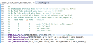
아래 캡처한 사진의 코드에서 GPIO10 GPIO11 으로 설정되 어있는데

GPIO10 / GPIO11에서 DAC 변환 신호가 출력되면 AFE031에 전달되는 것이 아닌가?

SPI 통신이 아닌 DAC 신호만으로 통신하는 것 아닌가?

boostxl_afe031_f28004x_dacmode

어떻게 동작시키는지 좀알려주세요.

통신신호 파형은 어떻고 afe031의 출력이 어떻게 나오는지 스코프로 캡처한 파형이 있다면 올려줄 수 있나요

It seems to me 

It seems that the dacmode firmware communicates with afe031 through the output of the DAC block.

In the code in the captured photo below, it is set to GPIO10 and GPIO11. 

If the DAC conversion signal is output from GPIO10 / GPIO11, isn't it transmitted to AFE031?

Isn't it communicating only with DAC signals, not SPI communication?

boostxl_afe031_f28004x_dacmode

Please tell me how it works.

What is the communication signal waveform and what is the output of afe031? Can you upload the waveform captured with a scope?

  • Hi Jungho,

    In the image you sent over, the GPIO10 and GPIO11 are configured as input signals, not output signals. They are simply reading the state of the test jumpers on the board, somewhere in the update loop / initialization, they are used to set the Test/Tx mode of the board

    Regards,

    Peter

  • SPI 통신 신호는 어떤 핀에서 나오는 것인가?

    GPIO 설정함수가 너무 많은데 특정지을 수 가 없다.

    SCLK 에 High signal을 보내면 통신 신호가 나오는지?

    What pin does the SPI communication signal come from?
    
    There are too many GPIO configuration functions, so I can't specify one.
    
    If I send a high signal to SCLK, does the communication signal come out?
  • Hi Jungho,

    You may find the SPI configuration in the hal_spi.c file. 

    Pasting the relevant section of the configuration below

    void InitAFESpiGpio()
    {
        EALLOW;
    
        // SPI_MOSI
        GPIO_SetupPinOptions(16, GPIO_INPUT, GPIO_ASYNC | GPIO_PULLUP);
        // SPI_MISO
        GPIO_SetupPinOptions(17, GPIO_INPUT, GPIO_ASYNC | GPIO_PULLUP);
        // SPI_CS
        GPIO_SetupPinOptions(57, GPIO_INPUT, GPIO_ASYNC | GPIO_PULLUP);
        // SPI_CLK
        GPIO_SetupPinOptions(56, GPIO_INPUT, GPIO_ASYNC | GPIO_PULLUP);
    
        GPIO_SetupPinMux(16, GPIO_MUX_CPU1, 1);
        GPIO_SetupPinMux(17, GPIO_MUX_CPU1, 1);
        GPIO_SetupPinMux(57, GPIO_MUX_CPU1, 1);
        GPIO_SetupPinMux(56, GPIO_MUX_CPU1, 1);
    
        EDIS;
    }

    In this example, the SPI FIFO is used to control the output of the SPI pins. The messages to the AFE should be directly written to the FIFO and the SPI module itself will handle the message transmission. There are some example waveforms in the boostxl user guide 

    https://www.ti.com/lit/ug/sbou223/sbou223.pdf

    Regards

    Peter

  • 보니까 AFE031의 경우 PWM 보다는 DAC가 노이즈가 적어서 DAC로 PLC 송신신호를 출력하는 것으로 보이는데,

    그전에 SPI 통신으로 AFE031에 송신신호를 보낸다는 것인가? SPI 통신 데이터 신호는 레지스터 설정만으로 끝인가?

    In the case of AFE031, it appears that the PLC transmission signal is output through the DAC because the DAC has less noise than the PWM.
    
    Before that, do you mean to send a transmission signal to AFE031 through SPI communication? Is the SPI communication DATA signal just a register setting?


  • 위의 AFE031 데이터시트를 보면 TX_FLAG 와 RX_FLAG를 사용해야 하는 것처럼 보인다. (AFE031의 47번,48번 핀)

    AFE031 데이터시트의 44페이지를 보더라도 TMS320F28x MCU GPIO 핀과 연결되어있으며, 이것에 대한 연결을 해봐야 한다고 생각한다.

    현재 사용하는보드는 LAUNCH-F280049C 보드이며,

    사용 펌웨어는 dacmode 이다.

    이 펌웨어에서 47번 ,48번에 연결하는 핀으로 보이는 핀은 아래 코드처럼 F280049C의 GPIO10(93번), GPIO0(79번) 번 핀이라고 보인다.

    위 코드사진을 올린 이유는 그런 내용을 파악하기가 어려워서 올린 것이다.

    다시한번 검토하고 회신주기 바란다.

    Looking at the AFE031 datasheet above, it looks like TX_FLAG and RX_FLAG should be used. (Pins 47 and 48 of AFE031)
    
    If you look at page 44 of the AFE031 datasheet, it is connected to the TMS320F28x MCU GPIO pin, and I think you need to connect to this.
    
    The board currently used is the LAUNCH-F280049C board.

    The firmware used is dacmode. The pins that appear to be connected to numbers 47 and 48 in this firmware appear to be pins GPIO10 (#93) and GPIO0 (#79) of F280049C, as shown in the code below.  The reason I uploaded the code photo above was because it was difficult to understand the contents. Please review again and reply.
  • Hi Jungho,

    I am currently out of office this week for US holiday, please expect a reply next week. Thanks

    Regards,

    Peter

  • Hi Jungho,

    I think there is miscommunication. Per the software/hardware user guide (https://www.ti.com/lit/ug/sbou223/sbou223.pdf) you can refer to transmitter example on how to send data. Specifically look at the Transmitter Example section. It details that a periodic interrupt is used to write a value from DMA data buffer register to the AFE031 through SPI. Then the AFE031 DAC output modulates the SunSpec output. So you are using the correct code. It may be helpful to initially test adjusting the DMA data buffer and changing some data that is being sent to the AFE031 to see the impact on the DAC output

    Regards,

    Peter