Other Parts Discussed in Thread: PMP23216, TMS320F280039C
Tool/software:
Hello,
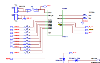
We are designing a 3kW DC/DC power converter based on the TIDM-02000 reference design, and we have encountered an issue during the aging experiment. The converter experiences a short circuit after running for about 30 minutes under full-load operating conditions.
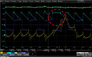
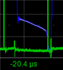
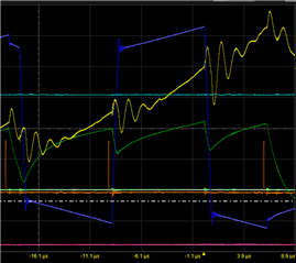
Below is a waveform captured just before the occurrence of the short circuit:
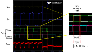
 <Control variable is Iinput, not Ipri>
<Fig. 1: Experimental results showing short circuit operation at full-load condition>
Blue waveform: Transformer primary current (Ipri).
Red waveform: Input current (I_Iinput)
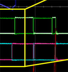
From Fig. 1, we observed that just before the short circuit, the pink gating signal fails to turn off earlier than the light green gating signal, as expected.
We suspect the short circuit is caused by insufficient slope compensation. Currently, the slope value is set to 13. We increased the slope compensation value to 23, which extended the operating time. However, the converter still tripped after a longer duration (Short circuit). So, we concluded that the slope compensation may still be inadequate, though other issues cannot be ruled out.
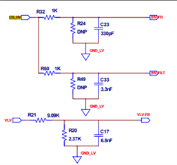
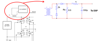
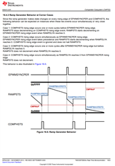
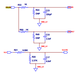
From the TI Design Note (PMP23216, Page 11), the following information about slope compensation is provided

![]()
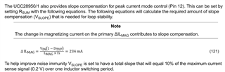
In another reference design (slua560d) (UCC28950 600W Phase Shifted Full Bridge Design Review/Application Report (Rev. D))
the slope value is determined based on change in the magnetizing current.

My specific queries are:
1. Could the short circuit phenomenon be caused by insufficient slope compensation?
2. Are the above formulas suitable for calculating the slope compensation ramp for TIDM-02000 based topology (Please note that Ipri is used as the control variable instead of the inductor current)?
3. After calculating slope in Amps/µs, how can this value be scaled and applied to generate the ramp in the DAC (range: 0–255 for an 8-bit DAC)?
4. Is there a more accurate or theoretical method to determine the required slope compensation value for PSFB?
We would greatly appreciate your guidance on calculating and applying the correct slope compensation value, as well as any insights into other potential causes of the short circuit.
Thank you in advance for your support.
Best Regards


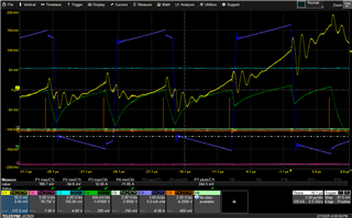


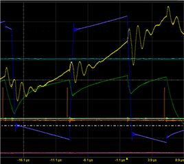
 <Blue: Itr(pri), Orange: