Part Number: F29H85X-SOM-EVM
Other Parts Discussed in Thread: SYSCONFIG
Tool/software:
Hi Team,
I've come across an ADC read error which i'm not sure how to solve. Essentually, reading any voltage,not GND or 3.3, produces a significant error. For example, when reading half scale 1.65 voltage, I get an output of 1.633 voltage which is around 1% error, but is significant for digital power applications.
Please see the methodology below:
Specs
- SOM rev E1 - connected to Adapter board + HSEC dock connector
- SDK 1.0.00 - Using ADC2_ex_soc_epwm
Vref Selection - Internal 3V3:
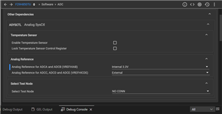
ADC input selection - A1
Vref Switches: POS1 Down
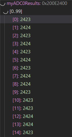
Input voltage measured: 1.650 V measured with Fluke Multimeter at HSECDOCK Connector pin 11
ADC measurement by C2000:
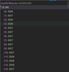
ADC Register input - 0x07EB = 1.63308105469 V
1) For the future, if the default configuration of the SDK examples is using the internal 3.3V pins, and the default configuration of the EVM switches is external 3.0V into the VREF device, there should be some clear documentation in the ADC example software that the switches must be changed.
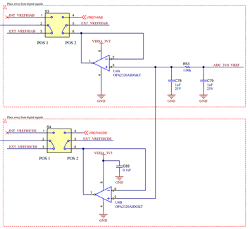
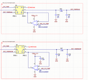
From Rev E1 to Rev A, we've made changes to the Vref circuity, could you please clarify why these changes were made and what benefit they have to the board design?