Part Number: TMS320F28P659DK-Q1
Tool/software:
Hi Champ,
I am asking for my customer.
They are designing the HW design with F28P659DK8PTPQ1 (176-pin) device.
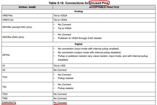
(1). May I reconfirm that pin 92, 146, 148 on this package could all be configured as the ERRORSTS Pin, correct ?
(2). If the pin 92, 146, 148 aren't expecting to be used as an ERRORSTS pin, saying to be used as a general input / output. From HW design, the external pulldown isn't a MUST need, right ?
(3). The pin 92, 146, 148 by default should all be set as GPIO (GPIO Muxed Pins, Reset = 0). In TRM, it specially mentions that
The ERRORSTS pin is tri-stated (high impedance) until the chip power rails ramp up to the lower operational limit.
The question is that aren't every single GPIO keeping as high impedance from device powers up until user manually configures the pin in main(), why we specially emphasize on this statement ? Any differences between ERRORSTS pin (pin 92, 146, 148) and normal GPIO pin ?
Thanks and regards,
Johnny