Part Number: TMS320F28P650DK
Tool/software:
Hi experts,
In the F28P65x_CLA_STL_API_User's_Guide.pdf

In the F28P65x_C28x_STL_API_User's_Guide.pdf

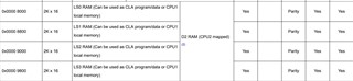
Both of CPU2 and CLA test need to use 0x8000. How to do the CPU2 & CLA test at the same time?
Thanks,
Leo