This thread has been locked.

If you have a related question, please click the "Ask a related question" button in the top right corner. The newly created question will be automatically linked to this question.

TMS320F280025C: SPI Clocking schemes in spi_ex6_eeprom.c

Part Number: TMS320F280025C

Tool/software:

Hello support team,

spi_ex6_eeprom.c is written to work with the SPI Serial EEPROM AT25128/256

AT25128 supports SPI Modes 0 (0,0) and 3 (1,1).

Why should we configure TMS320F280025C in mode 1(0,1)?

Should we always add half-cycle between master and slave?

I'd like to use https://www.ti.com/product/ADS131M02, which runs in mode 1,  in my application. Does that means I should configure TMS320F280025C in mode 0?

Thank you and best regards,

Quy

  • Quy,

    You should choose the configuration on the F28002x which matches what you need. Let me explain:

    The AT25128/256 datasheet has the following timing diagram, taken from microchip's website:

    AT25128/256 SPI Timing Diagram

    Notice that the SI/SO bits transmit a half-cycle ahead of the rising edge of the clock and sampled on the rising edge.

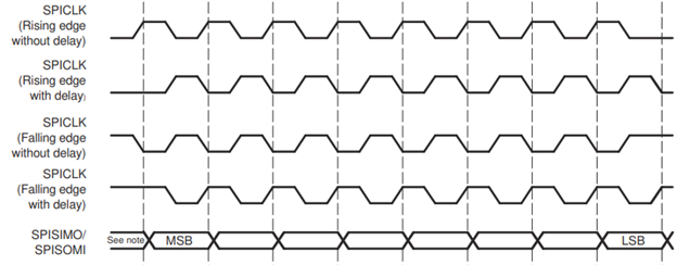
    Now, refer to the F28002x TRM Figure 27-7. SPICLK Signal Options, where the diagram shows, in order, modes 0, 1, 2, and 3:

    F28002x SPI Timing Diagram

    Notice Mode 1, where data is transmitted a half-cycle ahead of the rising edge of the clock and sampled on the rising edge. This matches the behavior of the AT25128/256, so that's what's used by our code.

    How the mode corresponds to the timing is not an exact standard, unfortunately. As long as each device samples the data bit at a point when it is in a stable state, there should be no loss of data. If you look at the ADS131MO2 datasheet section 8.5.1, it is expected that the data is transmitted on the rising edge and sampled on the falling edge of the clock, matching what the F28002x refers to as 'Rising edge without delay' (mode 0).

    Regards,
    Jason Osborn