This thread has been locked.

If you have a related question, please click the "Ask a related question" button in the top right corner. The newly created question will be automatically linked to this question.

UCC28950: Abnormal Oscillation During Burst Mode Transition 2

Guru 12295 points
Part Number: UCC28950


Tool/software:

Hi Mike,

Continuation of a related question.

You commented that you should check the following three things as countermeasures to the oscillation phenomenon.
1. Review the capacitance of Cout
2. Set Rtmin to 10kΩ and perform testing
3. Properly set the on/off control of the SR FET

I have a question about 1.

Current Conditions
・ESR=83.33mΩ
・VTRAN=600 mV
・Pout=600 W
・Vout=12V
・Efficiency η=0.9

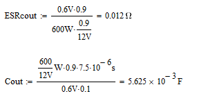
Based on the datesheet, we calculated the allowable ESR value for the output capacitor:

Calculation results : ESRCOUT450.54=0.012Ω=12mΩ

The current ESR value of 0.08333Ω (83.33mΩ) exceeds this limit, which may be too high. Could you please confirm if this calculation is correct?

I will also send you waveform information for your reference. Do you know the cause as shown in the attached waveform? If you find out the method to fix it, please let me know.
Full bridge waveform.xlsx

Thanks,

Conor

  • Hello,


    I double checked the Cout and ESRcout based on the information in the data sheet.  The calculation does calculate 12 mOhm.  So, if you used 83.33 mOhm you will have greater dv/dt to large signal transients caused by ESR.


    In regards to your waveforms on the gates of the FETs of your H Bridge.  Did you take these with a differential probe?


    Regards,

  • Hi Mike,

    Thank you for checking the calculation results.

    In regards to your waveforms on the gates of the FETs of your H Bridge.  Did you take these with a differential probe?

    Yes, they were measured with a differential probe.

    Thanks,

    Conor

  • Hello,


    If you took the gate waveforms with a differential probe that indicates that the noise is differential and may be coupling into the gate signal gate paths somehow.

    What is interesting about the waveforms is the C and D gate noise seems to occur at FET turn-on and the A and B gate noise does not occur when FETs A and B turn-on.  I am thinking the turn-on of FETs C and D are related to the turn on FETs C and D.  To verify if this is case could you take QA, QB, QC and QD gate waveforms on the same plot?  I want to see if they line up.


    Regards,

  • Hi Mike,

    To verify if this is case could you take QA, QB, QC and QD gate waveforms on the same plot?  I want to see if they line up.

    I have attached the gate waveforms I have obtained, so could you please take a look?

    Superimposed full bridge waveform.xlsx

    Thanks,

    Conor

  • Hello,


    I wanted you to retake the plots with the 4 gate waveforms on them.    You pasted one plot on top of the other.  This will not show if the noise synchronizes up.


    Please retake the FETs QA through QD gate on the same oscilloscope plot with a differential probe?


    We are doing this to see if the noise lines up the gates.  If it does it will narrow the noise source down to one source.


    Regards and Thanks,

  • Hi Mike,

    The waveforms measured at the same time were added to Excel.

    20250306_Superimposed full bridge waveform.xlsx

    Thanks,

    Conor

  • Hello,


    Thankyou for taking these waveforms.  The gate driver noise on A and B tracks the turn-on of FETs C and D.  This means the noise is occurring due to the QDd transitions.


    I think this noise is either on QDd or from the secondary rectifier inputs.  Cout you take waveforms of FET QDg, QDd and the secondary switch nodes at the same time?  I want to see which node is actually causing the ringing.  Once we figure that out we will be able to mitigate it.  


    Regards,

  • Hi Mike,

    Thanks for your reply. I got the waveform, can you check it?

    20250310_full bridge waveform.xlsx

    Thanks,

    Conor

  • Hello,


    Your inquiry has been received and will be answered in the order that it has been received.


    Regards,

  • Hello,


    Could you tell me what the waveforms are in the excel file?


    You were supposed to take the below waveforms.  There should have been 4 waveforms on one plot.  Please see below.

    “Cout you take waveforms of FET QDg, QDd and the secondary switch nodes at the same time? 


    We are trying to figure out where the noise comes from so we can mitigate it.

    Regards,

  • Hi Mike,

    ・QD G-S voltage (yellow waveform)
    ・QD D-S voltage (green waveform)
    ・Both ends of the transformer secondary winding (light blue)

    These three waveforms were acquired simultaneously and recorded in the Excel file 20250310_full bridge waveform.xlsx. Have you checked them?

    If the acquisition point of the waveform seems to be incorrect, please comment on which part should be measured based on the reference circuit diagram, etc.

    In particular, it is not clear what "secondary switch nodes" refers to, so my understanding may be incorrect. Currently we are measuring the voltage across the secondary winding of the transformer.

    Thanks,

    Conor

  • Hello,


    Thanks for the information and I will review the waveforms and get back to you with my recommendations.


    Regards,

  • Hi Mike,

    I apologize for the short notice, but we are in a bit of a hurry regarding this matter.
    Would it be possible to receive a response by the end of today (March 13)?
    We would greatly appreciate your prompt attention to this request.

    Thanks,

    Conor

  • Hello,


    I looked at the waveforms and it looks like noise is coupling in from the QDd switch node.

    This is most likely do to your layout and you may have traces close to the switch node that you should not.  Layout review is not a service provided on the e2e.


    In regards to the layout, I would recommend fallowing the layout guide lines in the data sheet.  However, you could evaluate the UCC28950EVM-442 600W reference design layout and compare it to yours.   I would recommend that you make layout similar to this.

    https://www.ti.com/tool/UCC28950EVM-442


    The following link will bring you to an application note on layout.  This was written for operational amplifiers but the layout techniques pertain to power supplies as well.  I believe this information will help you resolve your layout issues.

    https://e2echina.ti.com/cfs-file/__key/telligent-evolution-components-attachments/13-109-00-00-00-01-19-11/Circuit-Board-Layout-Techniques.pdf


    The last option is if you need this resolved in a timely fashion is to consult with a power supply design consultant to review your layout.  This may be the fasted way to resolve your issue.


    Regards,