This thread has been locked.

If you have a related question, please click the "Ask a related question" button in the top right corner. The newly created question will be automatically linked to this question.

TMS320F28379D: Unable to observe XCLKOUT signal on GPIO24 via XBAR routing

Part Number: TMS320F28379D


Tool/software:

Hello,

I am working on the F28379D and trying to route the XCLKOUT signal to an accessible GPIO pin using the XBAR fabric.

Since GPIO73 is configured for XCLKOUT, but not physically probe-able on my board, I tried the following routing:

XCLKOUT (via GPIO73) → InputXBAR1 → OutputXBAR1 → GPIO24

Below is the code I used (simplified):

#include "F2837xD_device.h"
#include "F2837xD_sysctrl.h"
#include "F2837xD_gpio.h"
#include "F2837xD_xbar.h"
void led(void);
void main(void) {

// Configure XCLKOUT source and divider
EALLOW; //
ClkCfgRegs.CLKSRCCTL1.bit.XTALOFF = 0; // Enable XTAL
ClkCfgRegs.CLKSRCCTL3.bit.XCLKOUTSEL = 2; // CPU2.sysclk as source
ClkCfgRegs.XCLKOUTDIVSEL.bit.XCLKOUTDIV = 1; // Divide by 2

GpioCtrlRegs.GPAGMUX1.bit.GPIO1 = 0;
GpioCtrlRegs.GPAMUX1.bit.GPIO1 = 0;
GpioCtrlRegs.GPADIR.bit.GPIO1 = 1;
GpioDataRegs.GPACLEAR.bit.GPIO1 = 0;


GpioCtrlRegs.GPAGMUX2.bit.GPIO16 = 0;
GpioCtrlRegs.GPAMUX2.bit.GPIO16 = 0;
GpioCtrlRegs.GPADIR.bit.GPIO16 = 0;
GpioCtrlRegs.GPAPUD.bit.GPIO16 = 1;

GpioCtrlRegs.GPCGMUX1.bit.GPIO73 = 1;
GpioCtrlRegs.GPCMUX1.bit.GPIO73 = 3;
GpioCtrlRegs.GPCDIR.bit.GPIO73 = 1;
// Configure Input XBAR to route GPIO73 (XCLKOUT)
InputXbarRegs.INPUTSELECTLOCK.bit.INPUT1SELECT = 0; // Unlock Input Select
InputXbarRegs.INPUT1SELECT = 73; // Route GPIO73 (49 in hexa) to InputXBAR1
InputXbarRegs.INPUTSELECTLOCK.bit.INPUT1SELECT = 1;

// Configure Output XBAR to route InputXBAR1 to GPIO24
OutputXbarRegs.OUTPUTLOCK.bit.LOCK = 0; // Unlock Output Select
OutputXbarRegs.OUTPUT1MUX0TO15CFG.bit.MUX1 = 1; // Route InputXBAR1 to MUX1 of Output1
OutputXbarRegs.OUTPUT1MUXENABLE.bit.MUX1 = 1;
OutputXbarRegs.OUTPUTLATCHENABLE.bit.OUTPUT1 = 0;
OutputXbarRegs.OUTPUTINV.bit.OUTPUT1 = 0;

// Configure GPIO24 for OutputXBAR function
GpioCtrlRegs.GPAGMUX2.bit.GPIO24 = 1;
GpioCtrlRegs.GPAMUX2.bit.GPIO24 = 1; //select as OUTPUTXBAR1
GpioCtrlRegs.GPADIR.bit.GPIO24 = 1; // Set as output
EDIS;
while(1)
{
led(); //just to check whether program is working
}


}
void led()
{
if (GpioDataRegs.GPADAT.bit.GPIO16 == 0) {
// Button is pressed (LOW), turn on the LED
GpioDataRegs.GPASET.bit.GPIO1 = 1;
} else {
// Button is not pressed (HIGH), turn off the LED
GpioDataRegs.GPACLEAR.bit.GPIO1 = 1;
}
}
 Observations:
  • The LED responds correctly to the button, which confirms the program is running.

  • All related registers (checked via Expressions window) are correctly set.

  • However, when I probe GPIO24 on the oscilloscope (with and without EDU MKII), I only see noise—no square wave or clock signal.

  • I’ve tried adjusting the XCLKOUT source and divider but still no signal is seen.

 Question:

Why is the signal not reaching GPIO24? Is the InputXBAR1 → OutputXBAR1 routing valid for this purpose, or am I missing something?

Any insights would be greatly appreciated!

Thank you,
Shivani

  • Hi Shivani, 

    I don't think this is a valid use-case for the INPUTXBAR specifically. See the statement below from the device TRM:

    The Input X-BAR simply connects the signal on the input buffer to the output of the selected Input X-BAR instance.

    This means that it is expecting a signal to be driven to the input buffer from external source. The connection route is valid, but since there isn't an external signal driving GPIO73, it is just routing whatever input signal that exists on that pin.

    You mentioned that the pin isn't accessible, what is it connected to on the board?

    I also just want to verify that you configured the proper mux mode (3) for GPIO73 to enable XCLKOUT on that pin.

    The expectation for this to work would require an external jumper/routing from GPIO73 to another available GPIO signal which you would then configure the inputxbar -> outputxbar route. Since the clock signal is being externally applied to the input buffer of the middle-man GPIO, the clock signal would then be routed to GPIO24.

    Best Regards,

    Zackary Fleenor

  • Thank you so much, Zackary!

    I had misunderstood the role of the Input XBAR — I assumed I could use it to route the internally generated XCLKOUT from GPIO73 back into the chip. As in the TRM, it is given that we've to route XCLKOUT via GPIO73.

    But GPIO73 is not accessible as it is present on a small dense structure which we cannot probe and route it using external jumper wires as it is that small.

    From the snapshots provided you can verify the configuration. 

    What should be done now?

    Regards 

    Shivani

    snaps_embedded.zip

  • Hello Shivani,

    One thing I noticed from the snapshots provided.

    You are setting the incorrect value for GPyGMUXn.GPIOz, this should be 0 instead of 1 to enable the XCLKOUT mux option.

    Can you try this?

    Can you also provide pictures of the board and any design files/schematics for reference so we can brainstorm possible solutions?

    Best Regards,

    Zackary Fleenor

  • Hi Fleenor.
    Thanks for noticing the issue. Let me try this and I'll let you know. 
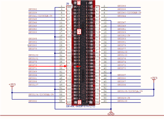
    Btw, I'm attaching launchpad Schematic. Also, picture of board, where the J9 is also highlighted.
    LAUNCHXL-F28379D 开发套件 | TI.com.cn - Here also, you can see the board details.
    Regards,
    Shivani

    Schematic.zip

  • Hey Shivani,

    I thought this was a custom board and didn't realize you were using the Launchpad HW.

    GPIO73 does come out on the J9 header here on pin 37.

    Additional details on this header can be found here: https://www.digikey.com/en/products/detail/hirose-electric-co-ltd/DF40C-60DP-0-4V-51/1969488

    The most important point to note is the 0.016" (0.40mm) pitch.

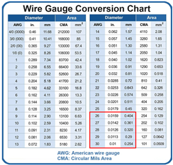
    If possible, you can solder on a small >=26 AWG jumper wire to the pcb pad footprint of pin 37 which could then be (very carefully) probed for the XCLKOUT signal after making the changes mentioned previously.

    There are many excellent tutorials on YouTube and other channels demonstrating this kind of PCB modification (See PCB Modification by Soldering SMT Jumpers).

    If it is possible to directly probe the GPIO73-XCLKOUT signal, then any XBAR configuration requirements become a moot point.

    Let us know your thoughts and if you are able to correctly observe XCLKOUT with the provided solution.

    Best Regards,

    Zackary Fleenor

  • Hi Zackary,

    Thanks for the detailed response and the solution you suggested.

    However, I wanted to check if there's any alternative way to access XCLKOUT without soldering, as unfortunately, I do not have the option to perform hardware modifications on the LaunchPad.

    To give more context — my project involves implementing a clock tree, where I need to observe various internal clock sources, analyze their stability, and compare them to evaluate clock skew or offset. That's why I’m specifically interested in tapping into the XCLKOUT signal for observation and analysis.

    Would there be a way to route or replicate the XCLKOUT signal through another accessible GPIO or subsystem without requiring external wiring?

    Appreciate your help and looking forward to any suggestions that could support this use case within the constraints of the board.

    Regards,
    Shivani

  • Hello Shivani,

    I have discussed this with other experts and I think I should correct a statement I made earlier.

    The IO Buffer in this device does support enabling both output (XCLKOUT) and input (INPUTXBAR) simultaneously to effectively create an internal loopback to OUTPUTXBAR and then to the output driver of another GPIO. After making the correction to the GPyGMUXn.GPIOz configuration, and retaining your previous xbar configuration are you still unable to see the XCLKOUT signal on GPIO24?

    Apologies for causing any confusion in regards to the INPUTXBAR and OUTPUTXBAR functionality. Your initial understanding was correct in this case.

    Best Regards,

    Zackary Fleenor