This thread has been locked.

If you have a related question, please click the "Ask a related question" button in the top right corner. The newly created question will be automatically linked to this question.

TMS320F280037C: CLB FSM internal timing logic

Part Number: TMS320F280037C
Other Parts Discussed in Thread: SYSCONFIG, C2000WARE

Tool/software:

Hi Champs,

I ask this for customer. Now customer tried to use CLB FSM to implement functions such as clock synchronization and latching. However, from the TRM, it can only be seen that the FSM module is timing-dependent state control, and the specific internal RTL level is not explained in detail.

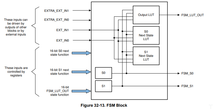
Now customer wants to know, can the following clock sync latch function be implemented? Do we have a configuration example and suggestion?

Thanks!


Best Regards,

Julia

  • Hi Julia,

    Yes the FSMs can be used as a latch by modifying the equations for the state bits in SysConfig. You can control the timing of when the latch output is updated using counter events. If there is no example similar to this in C2000Ware I can guide with the implementation.

    Thank you,

    Luke

  • Hi Luke,

    Now I work with customer and realize RS latch with below configuration.

    Customers also want to know, what is the real logical structure of this configured latch? Which of the following is similar? This is related to the key verification of the customer's design, please be sure to help confirm, thank you!

     (without clock)

     (with clock)

    Julia

  • Hi Luke,

    Customers also want to know, what is the real logical structure of this configured latch? Which of the following is similar? This is related to the key verification of the customer's design, please be sure to help confirm, thank you!

    Could you help to check this? Customers are now anxious to know this. Thanks!

    Julia

  • Hi Julia,

    Apologies for the delayed response.

    This diagram in the TRM outlines the functionality of the FSM:

    A look up table is used for each state bit using s0, s1, e0, and e1 as inputs. On each CLB Tile clock edge, the current s0 and s1 values are updated based on the output of the lookup table.

    Let me know if this answers your question on knowing the logical structure of the FSM.

    Thank you,

    Luke