Other Parts Discussed in Thread: THS4521, , TINA-TI
Tool/software:
- System Setup:
I am working on a Phase-Shifted Full-Bridge (PSFB) isolated DC-DC converter. For sensing the output voltage and inductor current, I’m using a Fully Differential Op-Amp (TI THS4521 SHKJ). The sensed signals pass through an RC filter (500 Ohms & 2nF) placed at the differential output of the op-amp before being connected to the ADC pins of a DSP (LaunchXL TMS320F28379D) configured in differential mode. My operating frequency is 300 kHz.- I trigger ePWM1 interrupt at TBPRD = 0 and use SOCA and SOCB at TBPRD/8 and TBPRD*5/8, respectively, to oversample and average the signal. I’d be happy to explain my reasoning behind this in more depth.
-
Problem Description:
The sensed signals are accurate only up to a certain voltage and current—approximately 120 V for voltage and 0.68 A for current.-
Voltage sensing: Beyond 120 V, the sensed signal begins to increase very slowly and seems to saturate, despite the actual voltage rising further.
-
Current sensing: Similar behavior is observed after 0.68 A, though the signal remains accurate up to around 170 V output.
I’ve already tried adding a buffer op-amp, but that didn’t help. Changing the RC filter’s cutoff frequency shifts the saturation point slightly but still gives the best results near 120–130 V. My goal is to sense up to 200 V reliably.
-
-
Questions I Have:
-
How does the RC filter at the ADC input affect the signal conditioning process, especially in differential mode sensing?
-
Could this behavior be due to an impedance mismatch between the op-amp and ADC input? If so, how does that manifest in this case?
-
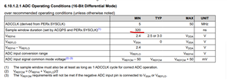
What acquisition period (ACQPS) should I consider ideal? I’ve tested values from 80 to 250. Currently, I’m using ACQPS = 120, and I can explain why I use this value in more detail if needed.
-
Is there anything in the interrupt generation process that you think I should look into further?
-