This thread has been locked.

If you have a related question, please click the "Ask a related question" button in the top right corner. The newly created question will be automatically linked to this question.

TMS320F28377D: ADC: DMA read of stale result

Part Number: TMS320F28377D


Tool/software:

Hi,

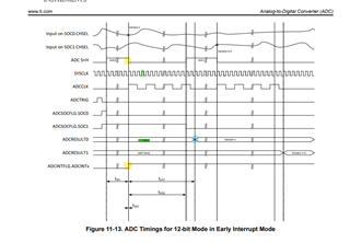
I've recently taken into account the Silicon errata sprz412n, and I'm having some difficulty understanding the point "ADC: DMA read of stale result", especially in terms of visualizing the scheduling.

From what I understand in the details section, the ADCINT is triggered before the end of the acquisition, which could result in stale data from the previous cycle. Am I correct in saying that this only affects the data of the SOC that generates the ADCINT (and the subsequent SOCs—but that wouldn't be considered abnormal behavior)?

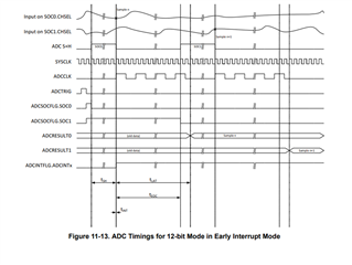
What’s confusing for me is the Workarounds section. Using a "dummy DMA" to introduce a delay seems a bit extreme, which makes me think I may not fully understand the advisory.

Since we’re already using all DMA channels but not all ADC SOCs, we’re considering using a "dummy SOC" to trigger the ADCINT signal that, in turn, triggers the DMA. Can you please confirm that this is a correct workaround ?

Best regards , BR

  • Hello,

     "Dummy DMA" a delay is used as a way to introduce a delay between the ADCINT interrupt and the actual DMA transfer. This delay allows the ADC to complete the acquisition and ensure that the data is valid before the DMA reads it.

    I think your workaround with "dummy SOC" is good alternative and should work as well. Let me loop in DMA expert to get another confirmation on this.

    Best regards

  • Hi Bruno,

    I apologize for the delay on this. I'm assuming you're using 12-bit ADC mode with early interrupt mode as you've shown in the timing diagram screenshot.

    To clarify, the ADCINT is triggered at the very end of the acquisition window (see yellow highlighted portion), however the results aren't latched in the result register at this point. The are latched many SYSCLK cycles later (see the blue highlighted portion). The issue is that the DMA can read the result register (at earliest) 3 SYSCLK cycles after the S + H window is complete (see green highlighted portion), at which point the new data is not latched in the result register yet. 

    Am I correct in saying that this only affects the data of the SOC that generates the ADCINT (and the subsequent SOCs—but that wouldn't be considered abnormal behavior)?

    This is correct. It isn't so much "abnormal" behavior as something you would just need to account for in your application (and requires a less intuitive solution than most DMA+peripheral implementations due to the timing). In newer devices we have fixed this issue. 

    The dummy SOC you've mentioned should work. You would just need to configure the DMA interrupt to trigger at the end of SOC1's S+H window but have the DMA read the ADCRESULT0 register so that the SOC0 data is latched when by the time the DMA accesses it.

    Please upvote this response if it answers your question. Slight smile

    Best Regards,

    Delaney

  • Hi Delaney,

    I thank you for the answer and especially for the detailed diagram 

    BR