Other Parts Discussed in Thread: SYSCONFIG, UNIFLASH
Tool/software:
Hey group.
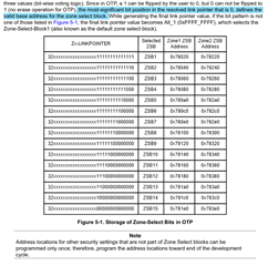
Figure 5-1 does not represent the blue highlighted text, states MSB position represents offset address, not LSB. Figure 5-1 is draw backwards to what is written of how a link pointer is made valid. What the table shows is to modify LSB bits 1 to 0 because they all start out as 1's in the OTP. Fig. 5-1 link pointer bit positions are drawn backwards, LSB to MSB. If the text is wrong, then it needs to be corrected to match Fig.5-1 indicate LSB bits (1) must be changed to (0) in the OTP, not state MSB.
Logically it would make sense to change high order (1) bits in descending order for GEL code to work correctly. The x49c GEL ends up 0x00000000 and targets pointer block offset addresses perfectly.
The table should represent after the fact of modified link pointers (LP) being they are critical for DCSM peripheral working correctly. Either change all the 0's to 1's and 1's to 0's or fix the text to state LSB in ascending order up to MSB bit positions as to elaborate what is being implied by Fig.5-1 for critical OTP bits being changed.
Seemingly it destroys DCSM LP's bits recognition if the MSB is made (0) before LSB has been first changed, x49c DCSM. Perhaps add the words LSB ascending or MSB descending so the reader knows what, why and how. Frankly it doesn't seem logical to modify bits from LSB to MSB in an existing OTP Dword anyway, unless maybe you are Russian. Perhaps DCSM peripheral reads LP's LSB to MSB? Readers have no idea what or why the figure is backwards to the blue text stated first MSB made (0). Noted x49c DCSM if three link pointers of a zone are not made exact same binary value, the LP1 error flag is raised MSB bit position of the changed bit that is not same as LP1. Once all three LP's are made to match, the LP error flag is dropped.