This thread has been locked.

If you have a related question, please click the "Ask a related question" button in the top right corner. The newly created question will be automatically linked to this question.

F29H85X-SOM-EVM: ADC SOC Trigger source - GPIO

Part Number: F29H85X-SOM-EVM

Tool/software:

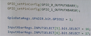
The ADC SOC trigger source is configured as InputXbar5, but the SOC is not being issued to the ADC, even though the InputXbar signal is functioning correctly (verified using OutputXbar and confirmed on the CRO).

and when configured external interrupt it is not being configured (XINT2) (registers being unwritten). how to solve this issue.

  • Hi Shashank,

    Can you share snippet of ADC and GPIO codes that set up the external SOC trigger for the ADC?

    Thanks,

    Joseph

  • Gpio 16 is configured as EPWM_9A output, and mapped to input cross bar 5th pin. input x bar 5th pin mapped to GPIO1 through output x bar and verified in CRO.

  • I'm using driverlib functions and I am able to trigger ADC conversions with External GPIO via INPUTXBAR5.  For my case, I used EPWM1A to toggle GPIO0 by configuring TBCTR and CMPA. Also verified that GPIO0 is toggling for the period set in TBCTR through an oscilloscope.  Check that the following registers (use register view in CCS) have the correct values to confirm that the bitfield statements are indeed writing to the registers:

         - InputXbarRegs.INPUTSELECT4 = the GPIO# that is toggling ( for your case this should be equal to 16 for GPIO16 )

         - ADCSOC0CTL.TRIGSEL = 4; (using INPUTXBAR5 for GPIO trigger)

    You are probably missing some steps in your set up.

    Regards,

    Joseph

  • Hello Joseph,

    Yes you are correct, I am mapped GPIO to the 6th input of the input cross bar (InputXbarRegs.INPUTSELECT[5]).

    when I trying to load multi core environment with flash configuration while writing the CPU3 program (0x10400000, Flash read interface-2, Read Port 0) it is throwing invalid address error. when CPU1 and CPU2 programs Flashed through Flash Read interface-0(FRI-0) working properly, how to resolve this issue .( when CPU3 program loaded through FRI1 it is loading properly but its program should be run in RAM, i need to run program in flash it self).

    Thanks, Best Regards.

    Shashank

  • Hi Shashank,

    I'm closing this post as it is categorized under ADC and it seems that you have fixed your issue on external GPIO trigger for the ADC.  For the other issue that you have raised, please post that under a different topic (possibly under Flash Bank Management) and it will be addressed accordingly.

    Regards,

    Joseph