This thread has been locked.

If you have a related question, please click the "Ask a related question" button in the top right corner. The newly created question will be automatically linked to this question.

LAUNCHXL-F280039C: SCI Serial Programmer not working

Part Number: LAUNCHXL-F280039C
Other Parts Discussed in Thread: C2000WARE,

Tool/software:

Good day, 

I am reaching out to see if someone can help me figure out why my firmware update is not working. 

1 - In the C:\ti\C2000Ware_5_04_00_00\driverlib\f28003x\examples\flash folder I built the flash_kernel_ex3_sci_flash_kernel and flashed it to both BANK0_LDFU and BANK1_LDFU build configurations. 

2 - I modified the flashapi_ex5_lfu_no_reset project found in the C:\ti\C2000Ware_5_04_00_00\driverlib\f28004x\examples\flash to work on a f28003x LAUNCHXL board. There are 2 builds, one for BANK0 and one for BANK1.

Modifications made are: 

Changed name of project to "flashapi_ex5_lfu_no_reset_F200839C".

Under project properties, I made all properties for the f28003x board the same as the f28004x except I changed the paths for the variables:
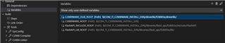
The C2000 Complier:

The C2000 Linker:

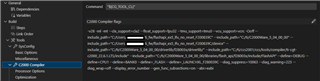
Under C2000 Complier, Pre defined symbols I added _LAUNCXL_F280039C so I could use the correct pins for LEDs and SCI TX and RX (LEDs are 20 22, SCI are 28 and 29).

I then flashed both projects to board. All flashes were set to erase necessary settings only:

The cmd files for Bank0 build and Bank1 build had to be modified so it would work with the F280039C, but the addresses are similar. 

I then built the both configurations and flashed to board. 

3 - I then used the flash_kernel_ex3_sci_flash_kernel to create a text output file. I build that in the CPU1_RAM configuration. I placed that file in the same folder as the serial programmer at C:\ti\C2000Ware_5_04_00_00\utilities\flash_programmers\serial_flash_programmer

4 - I then copied the text file from one of the modified flashapi_ex5_lfu_no_reset builds and pasted it in the same folder as the serial programmer. 

5 - I opened a command prompt and directed it to the serial programmer directory at C:\ti\C2000Ware_5_04_00_00\utilities\flash_programmers\serial_flash_programmer.

6 - then entered serial_flash_programmer.exe -d f28003x -k flash_kernel_ex3_sci_flash_kernel.txt -a flashapi_ex5_lfu_no_reset_F200839C.txt -b 9600 -p COM8 -v  and pressed enter.
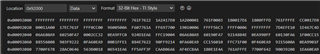
I got this output:

Can someone help me with what may be going wrong? Or any tips to try to get this to work?

Cheers,

Scott

  • Hi,

    Our Flash kernel SME is OOO will be back on Monday. Please expect delay in response.

    Regards,

    Rajeshwary

  • Hi Scott,

    What is your desired behavior here? Do you want to boot via SCI and load the kernel to RAM and then perform a firmware upgrade? Or do you want to boot to flash (Bank0 or Bank1 build of LFU project) and perform a firmware upgrade? When using the latter option, you should be using serail_flash_programmer_appIn.exe so the host doesn't try and send the RAM-based kernel. The RAM-based kernel only needs to be sent if you're using the SCI boot mode.

    Have you taken a look at this guide? The document walks through setting up the project and how it should be run.

    Based on the output of the host programmer, I suspect there is a GPIO mismatch in your SCI configuration. 

    Kind regards,

    Skyler

  • Hi Skyler, 

    I am trying to load the kernel to RAM and then perform the firmware upgrade using the JTAG connection.

    I have taken a look at the guide, specifically section 6.2. I am using a LAUNCHXL-F280039C instead of a F28004x control card but making the assumption that it should work the same. 

    I will double check the SCI GPIOs.

    To confirm, switch 3 (S3) GPIO 24 needs to be set to '0' and GPIO 32 needs to be set to '1' to perform a SCI boot at all times?

    Cheers, 

    Scott

  • Hi Scott,

    I am trying to load the kernel to RAM and then perform the firmware upgrade using the JTAG connection.

    Can you clarify here? How are you loading the kernel to RAM? Through bootROM? This project shows how live firmware upgrades can be performed over SCI. The LFU solution is flash-based, so you don't need to load the kernel to RAM. The LFU solution is intended to be used by booting to flash and then performing the firmware upgrade over SCI. A flash kernel is used to perform firmware upgrades in the SCI boot mode where the bootloader does not reside in flash. 

    Can you provide a high-level overview of what your desired implementation is? There is some confusion on my end on which solution is best suited for this. 

    Kind regards,

    Skyler

  • Hi Skyler,

    I have been building the flash kernel (flash_kernel_ex3_sci_flash_kernel) in the f28003x flash examples in the CPU1_RAM build configuration and then opening a terminal and sending " serial_flash_programmer.exe -d f28003x -k flash_kernel_ex3_sci_flash_kernel.txt -a flashapi_ex5_lfu_no_reset_F200839C.txt -b 9600 -p COM8 -v". Not sure if this is loading the flash kernel to RAM.

    I am trying to understand how to perform a firmware update using SCI. The goal was to use examples to better understand how firmware updates work over SCI. I modified the flashapi_ex5_lfu_no_reset project from f28004x examples to work on the LAUNCHXL-F280039C dev board. However, if there is more straightforward way of doing a simple firmware update with another example I would like to hear it.

    I want to understand how to do a LFU with reset and without reset. From reading the documentation, a LFU with reset would be simpler so I will start there. 

    I want to run an application, do a firmware update and switch to the latest firmware with minimal downtime.

    Cheers,

    Scott 

  • Hi Scott,

    Thank you for clarifying! 

    I have been building the flash kernel (flash_kernel_ex3_sci_flash_kernel) in the f28003x flash examples in the CPU1_RAM build configuration and then opening a terminal and sending " serial_flash_programmer.exe -d f28003x -k flash_kernel_ex3_sci_flash_kernel.txt -a flashapi_ex5_lfu_no_reset_F200839C.txt -b 9600 -p COM8 -v". Not sure if this is loading the flash kernel to RAM.

    Yes, loading the kernel through bootROM will place the kernel in RAM. This application note discusses the flash kernels and how they are used to perform firmware upgrades from RAM (figure 1-1 explains the flow at a high-level). This is a more basic example of a firmware upgrade over SCI, so this is a good starting point. But, this is a different approach than what is used in the LFU examples. The key difference is that the kernel needs to boot via SCI, and the LFU solutions boot to flash and branch back to a bootloader when a firmware upgrade needs to be performed. They are different solutions. Hope this provides some clarity on what each solution should be used for.

    Since your end goals is to perform a live firmware update without reset, I'd suggest starting with the LFU with reset example because it is simpler. In this case, you won't have to load the kernel to RAM via SCI because it will have already been flashed to the device as part of the LFU with reset example. 

    Kind regards,

    Skyler

  • Hi Skyler, 

    Thank you for clarifying. I have to use the bootloader in flash, not RAM to perform a LFU.

    For a LFU with reset, will I have to flash the LAUNCHXL-F280039C with the sci flash kernel (flash_kernel_ex3_sci_flash_kernel) for each of the 3 build configurations, BANK0_LDFU, BANK1_LDFU, and BANK2_LDFU? This will load the flash kernel to the beginning of the flash bank.

    After that, can I load an example project (i.e. led_ex1_blinky) to the flash? Build the project in CCS and use the output txt file. 

    Then can I open a terminal and send "serial_flash_programmer.exe -d f28003x -k flash_kernel_ex3_sci_flash_kernel.txt -a led_ex1_blinky.txt -b 9600 -p COMX -v"?

    In the serial flash programmer line that will be sent using a terminal, with regards to the "flash_kernel_ex3_sci_flash_kernel.txt" portion, is this the text file that is created when I build it in CCS for the specific flash Bank? For example, if I want to program flash Bank 0 with code, I would have to build BANK0_LDFU and use the text file that was created in that particular build directory?

    Also, I have the switch 3 (S3) pins set on the Dev board as follows:

    GPIO 24 -> 0

    GPIO 32 -> 1

    Is this correct? 

    Cheers, 

    Scott

  • Hi Scott,

    For a LFU with reset, will I have to flash the LAUNCHXL-F280039C with the sci flash kernel (flash_kernel_ex3_sci_flash_kernel) for each of the 3 build configurations, BANK0_LDFU, BANK1_LDFU, and BANK2_LDFU? This will load the flash kernel to the beginning of the flash bank.

    Yes, this is correct.

    After that, can I load an example project (i.e. led_ex1_blinky) to the flash? Build the project in CCS and use the output txt file.

    Yes, but make sure the example project is using the expected flash bank. For example, the bank 1 example application should be built using a linker file that places all initialized sections in bank 1.

    Then can I open a terminal and send "serial_flash_programmer.exe -d f28003x -k flash_kernel_ex3_sci_flash_kernel.txt -a led_ex1_blinky.txt -b 9600 -p COMX -v"?

    Yes, this is correct.

    In the serial flash programmer line that will be sent using a terminal, with regards to the "flash_kernel_ex3_sci_flash_kernel.txt" portion, is this the text file that is created when I build it in CCS for the specific flash Bank? For example, if I want to program flash Bank 0 with code, I would have to build BANK0_LDFU and use the text file that was created in that particular build directory?

    Yes, the kernel text file is a result of building the project in CCS. When using the serial_flash_programmer.exe, this file (preceded by the -k option) will be sent immediately. This feature is used to load RAM-based kernels via bootROM, so you won't need to use it. Thus, you should use the serial_flash_programmer_appIn.exe. This -k option is still required (for now), but it won't actually be sent because this exe is assuming a flash-based kernel is already executing. We are removing this -k requirement in a future version of the serial_flash_programmer_appIn.exe.

    Also, I have the switch 3 (S3) pins set on the Dev board as follows:

    For flash boot mode, both pins should be set to 1. See table 4-4 of the TRM for details.

    Kind regards,

    Skyler

  • Hi Skyler, 

    Thank you for clarifying and answering my questions.  

    I am making progress. The menu appears and the application is downloading to flash. 

    However, I believe I may be not correctly configuring the flash cmd file.

    For simplicity and for me to better understand what is happening,  I am trying to load the originally led_ex1_blinky into Bank0 and then make a small modification to the blink period and flash that to BANK1. 

    I get the below menu now and enter '8' and press enter. 

    The application is downloaded and I get the below menu again:

    I enter 6 and press enter. Then it asks for a hex value to branch to and I enter 0x090002 and nothing happens. 

    For Bank0 I use the flash linker cmd file that was originally with the project as shown below. For Bank1, I change the BEGIN origin from 0x00080000 to 0x00090000 and "FLASH_BANK1_SEC0  : origin = 0x090000, length = 0x001000" to "FLASH_BANK1_SEC0  : origin = 0x090002, length = 0x000FFE" and also in the "SECTIONS" I change anything that has BANK0 to BANK1. 

    MEMORY
    {
       BEGIN            : origin = 0x00080000, length = 0x00000002
       BOOT_RSVD        : origin = 0x00000002, length = 0x00000126

       RAMM0            : origin = 0x00000128, length = 0x000002D8
       RAMM1            : origin = 0x00000400, length = 0x000003F8
       // RAMM1_RSVD       : origin = 0x000007F8, length = 0x00000008 /* Reserve and do not use for code as per the errata advisory "Memory: Prefetching Beyond Valid Memory" */

       RAMLS0           : origin = 0x00008000, length = 0x00000800
       RAMLS1           : origin = 0x00008800, length = 0x00000800
       RAMLS2           : origin = 0x00009000, length = 0x00000800
       RAMLS3           : origin = 0x00009800, length = 0x00000800
       RAMLS4           : origin = 0x0000A000, length = 0x00000800
       RAMLS5           : origin = 0x0000A800, length = 0x00000800
       RAMLS6           : origin = 0x0000B000, length = 0x00000800
       RAMLS7           : origin = 0x0000B800, length = 0x00000800

       RAMGS0           : origin = 0x0000C000, length = 0x00001000
       RAMGS1           : origin = 0x0000D000, length = 0x00001000
       RAMGS2           : origin = 0x0000E000, length = 0x00001000
       RAMGS3           : origin = 0x0000F000, length = 0x00000FF8
       // RAMGS3_RSVD      : origin = 0x0000FFF8, length = 0x00000008 /* Reserve and do not use for code as per the errata advisory "Memory: Prefetching Beyond Valid Memory" */

       BOOTROM          : origin = 0x003F8000, length = 0x00007FC0
       SECURE_ROM       : origin = 0x003F2000, length = 0x00006000

       RESET            : origin = 0x003FFFC0, length = 0x00000002

       /* Flash sectors */
       /* BANK 0 */
       FLASH_BANK0_SEC0  : origin = 0x080002, length = 0x000FFE
       FLASH_BANK0_SEC1  : origin = 0x081000, length = 0x001000
       FLASH_BANK0_SEC2  : origin = 0x082000, length = 0x001000
       FLASH_BANK0_SEC3  : origin = 0x083000, length = 0x001000
       FLASH_BANK0_SEC4  : origin = 0x084000, length = 0x001000
       FLASH_BANK0_SEC5  : origin = 0x085000, length = 0x001000
       FLASH_BANK0_SEC6  : origin = 0x086000, length = 0x001000
       FLASH_BANK0_SEC7  : origin = 0x087000, length = 0x001000
       FLASH_BANK0_SEC8  : origin = 0x088000, length = 0x001000
       FLASH_BANK0_SEC9  : origin = 0x089000, length = 0x001000
       FLASH_BANK0_SEC10 : origin = 0x08A000, length = 0x001000
       FLASH_BANK0_SEC11 : origin = 0x08B000, length = 0x001000
       FLASH_BANK0_SEC12 : origin = 0x08C000, length = 0x001000
       FLASH_BANK0_SEC13 : origin = 0x08D000, length = 0x001000
       FLASH_BANK0_SEC14 : origin = 0x08E000, length = 0x001000
       FLASH_BANK0_SEC15 : origin = 0x08F000, length = 0x001000

       /* BANK 1 */
       FLASH_BANK1_SEC0  : origin = 0x090000, length = 0x001000
       FLASH_BANK1_SEC1  : origin = 0x091000, length = 0x001000
       FLASH_BANK1_SEC2  : origin = 0x092000, length = 0x001000
       FLASH_BANK1_SEC3  : origin = 0x093000, length = 0x001000
       FLASH_BANK1_SEC4  : origin = 0x094000, length = 0x001000
       FLASH_BANK1_SEC5  : origin = 0x095000, length = 0x001000
       FLASH_BANK1_SEC6  : origin = 0x096000, length = 0x001000
       FLASH_BANK1_SEC7  : origin = 0x097000, length = 0x001000
       FLASH_BANK1_SEC8  : origin = 0x098000, length = 0x001000
       FLASH_BANK1_SEC9  : origin = 0x099000, length = 0x001000
       FLASH_BANK1_SEC10 : origin = 0x09A000, length = 0x001000
       FLASH_BANK1_SEC11 : origin = 0x09B000, length = 0x001000
       FLASH_BANK1_SEC12 : origin = 0x09C000, length = 0x001000
       FLASH_BANK1_SEC13 : origin = 0x09D000, length = 0x001000
       FLASH_BANK1_SEC14 : origin = 0x09E000, length = 0x001000
       FLASH_BANK1_SEC15 : origin = 0x09F000, length = 0x001000

      /* BANK 2 */
       FLASH_BANK2_SEC0  : origin = 0x0A0000, length = 0x001000
       FLASH_BANK2_SEC1  : origin = 0x0A1000, length = 0x001000
       FLASH_BANK2_SEC2  : origin = 0x0A2000, length = 0x001000
       FLASH_BANK2_SEC3  : origin = 0x0A3000, length = 0x001000
       FLASH_BANK2_SEC4  : origin = 0x0A4000, length = 0x001000
       FLASH_BANK2_SEC5  : origin = 0x0A5000, length = 0x001000
       FLASH_BANK2_SEC6  : origin = 0x0A6000, length = 0x001000
       FLASH_BANK2_SEC7  : origin = 0x0A7000, length = 0x001000
       FLASH_BANK2_SEC8  : origin = 0x0A8000, length = 0x001000
       FLASH_BANK2_SEC9  : origin = 0x0A9000, length = 0x001000
       FLASH_BANK2_SEC10 : origin = 0x0AA000, length = 0x001000
       FLASH_BANK2_SEC11 : origin = 0x0AB000, length = 0x001000
       FLASH_BANK2_SEC12 : origin = 0x0AC000, length = 0x001000
       FLASH_BANK2_SEC13 : origin = 0x0AD000, length = 0x001000
       FLASH_BANK2_SEC14 : origin = 0x0AE000, length = 0x001000
       FLASH_BANK2_SEC15 : origin = 0x0AF000, length = 0x000FF0

    // FLASH_BANK0_SEC15_RSVD     : origin = 0x0AFFF0, length = 0x000010  /* Reserve and do not use for code as per the errata advisory "Memory: Prefetching Beyond Valid Memory" */

    }


    SECTIONS
    {
       codestart        : > BEGIN, ALIGN(8)
       .text            : >> FLASH_BANK0_SEC2 | FLASH_BANK0_SEC3 | FLASH_BANK0_SEC4,   ALIGN(8)
       .cinit           : > FLASH_BANK0_SEC1,  ALIGN(8)
       .switch          : > FLASH_BANK0_SEC1,  ALIGN(8)
       .reset           : > RESET,                  TYPE = DSECT /* not used, */

       .stack           : > RAMM1

    #if defined(__TI_EABI__)
       .init_array      : > FLASH_BANK0_SEC1,  ALIGN(8)
       .bss             : > RAMLS5
       .bss:output      : > RAMLS3
       .bss:cio         : > RAMLS0
       .data            : > RAMLS5
       .sysmem          : > RAMLS5
       .const           : > FLASH_BANK0_SEC4,  ALIGN(8)
    #else
       .pinit           : > FLASH_BANK0_SEC1,  ALIGN(8)
       .ebss            : > RAMLS5
       .esysmem         : > RAMLS5
       .cio             : > RAMLS0
       .econst          : > FLASH_BANK0_SEC4,  ALIGN(8)
    #endif

        ramgs0 : > RAMGS0
        ramgs1 : > RAMGS0

        /*  Allocate IQ math areas: */
       IQmath           : > FLASH_BANK0_SEC1, ALIGN(8)
       IQmathTables     : > FLASH_BANK0_SEC2, ALIGN(8)

       .TI.ramfunc      : LOAD = FLASH_BANK0_SEC1,
                          RUN = RAMLS0,
                          LOAD_START(RamfuncsLoadStart),
                          LOAD_SIZE(RamfuncsLoadSize),
                          LOAD_END(RamfuncsLoadEnd),
                          RUN_START(RamfuncsRunStart),
                          RUN_SIZE(RamfuncsRunSize),
                          RUN_END(RamfuncsRunEnd),
                          ALIGN(8)

    }
    Could you explain how this file should be changed for BANK0 and BANK1? From my limited experience with bootloaders, I think I may be writing the application firmware over the bootloader? Do only flash addresses need to be changed or do RAM addresses also need to be changed? 
    Cheers, 
    Scott
  • Hi Scott,

    Your modifications to the linker file to store the led blinky in Bank 1 vs Bank 0 are correct. However, your branching address should be 0x90000, not 0x90002. A good way to double-check what is being programmed and where is by looking in the Memory Browser. You should see the led blinky programmed to Bank 1 after completing the DFU command. Additionally, if you plan to keep a version of the bootloader in the beginning of both flash banks, you should not store the LED blinky in the same area of Bank 0/1 that is reserved for the bootloader. Otherwise you will overwrite it, as you mentioned above.

    Initialized output sections that are stored in flash need to be updated to reflect the change from Bank 0 -> Bank 1. Uninitialized memory sections stored in RAM don't need to be modified but you should verify that the bootloader and application aren't sharing the same RAM address space during run-time. 

    Kind regards,

    Skyler

  • Hi Skyler,

    When I look in the Memory Browser, the data in address 0x00092000 is not correct. According to the "Live Firmware Update With Device Reset on C2000 MCUs" document I should see 5A5A 5A5A 5A5A 5A5A (START) 5B5B 5B5B (KEY) and then a 16 bit value to indicate the REV. I am getting values below:

    When I flash the dev board with the application using CCS, I get the same values in the same addresses. Not sure if the application is writing over the START, KEY, and REV values. 

    Should I change the address values in Bank1 Section2? Make a gap in the flash memory for the START, KEY, and REV values?

    Also, the serial flash kernel for BANK0 flash is divided up as below: Should the application flash (led_ex1_blinky) be the same values for SECTION 0 and SECTION 1? 

       BANK0_SEC1        : origin = 0x081000, length = 0x000017
       /* BANK 0 */
       FLASH_BANK0_SEC0  : origin = 0x08004C, length = 0x000FB4
       FLASH_BANK0_SEC1  : origin = 0x081017, length = 0x000FE9
       FLASH_BANK0_SEC2  : origin = 0x082000, length = 0x001000
       FLASH_BANK0_SEC3  : origin = 0x083000, length = 0x001000
       FLASH_BANK0_SEC4  : origin = 0x084000, length = 0x001000
       FLASH_BANK0_SEC5  : origin = 0x085000, length = 0x001000
       FLASH_BANK0_SEC6  : origin = 0x086000, length = 0x001000
       FLASH_BANK0_SEC7  : origin = 0x087000, length = 0x001000
       FLASH_BANK0_SEC8  : origin = 0x088000, length = 0x001000
       FLASH_BANK0_SEC9  : origin = 0x089000, length = 0x001000
       FLASH_BANK0_SEC10 : origin = 0x08A000, length = 0x001000
       FLASH_BANK0_SEC11 : origin = 0x08B000, length = 0x001000
       FLASH_BANK0_SEC12 : origin = 0x08C000, length = 0x001000
       FLASH_BANK0_SEC13 : origin = 0x08D000, length = 0x001000
       FLASH_BANK0_SEC14 : origin = 0x08E000, length = 0x001000
       FLASH_BANK0_SEC15 : origin = 0x08F000, length = 0x001000

    Cheers,

    Scott

  • Hi Scott,

    Yes, your application linker file should not be storing the program where the START, KEY, and REV values are placed. For your application linker sections, you don't need to update the memory sections. You just need to make sure the output sections are not mapped to memory that overlaps with the kernel/LFU reserved sections. You can update the memory sections if you want, but they won't affect the .out file unless you map an output section to them.

    Kind regards,

    Skyler

  • Hi Skyler, 

    When I build the led_ex1_blinky in CCS and load to the LAUNCHXL-F280039C dev board, the project loads into Flash at Section 2 as shown in the picture below and the LED does blink. 

    I then duplicated the flash linker file and made modifications to make a BANK1 copy. Changed the BEGIN origin: to 0x00090000, changed the FLASH_BANK1_SEC0 origin to 0x090002, length = 0x000FFE. and in the "SECTIONS" area of the file changed all "BANK0" to BANK1". I then built both build configurations for BANK0 and BANK1. 

    I then loaded only BANK0 and BANK1 sci serial flash kernel to the Dev board using CCS. Then I copied the BANK0 serial flash kernel text file and the BANK0 Blinky example text file to the serial flash programmer folder and ran the following command in terminal: "serial_flash_programmer_appln.exe -d f28003x -k flash_kernel_ex3_sci_flash_kernel.txt -a led_ex1_blinky.txt -b 9600 -p COM8 -v". Menu appeared, pressed '8' for Live DFU and when the download was complete I press '7' for reset CPU1. The LED does not blink. When I look at memory using CCS (debugging BANK2_LDFU from the sci flash programmer) , the memory looks as follows:

    the 3rd and 4th word are F's instead of data as shown when I use CCS to program the dev board.

    If I run the BANK0 serial flash kernel and the BANK0 blinky example application again and look at the memory it looks like below. The 0x00082000 address doesn't change but the 0x00092000 address shows the REV, START, and KEY:

    If I now run the BANK1 sci serial flash kernel and the BANK1 blinky example: I get the following in both 0x00082000 and 0x00092000 addresses.

    The first 4 words shows the REV, START, and KEY. The first 4 words of the application when comparing it to when I loaded the board using CCS is missing. 

    If I now go back and run BANK0 serial flash kernel and BANK0 blinky example application, the memory looks like below:

    I can flash back and forth between BANK0 and BANK1 and the REV seems to decrement correctly. However, the first 4 words of the application is missing. I am not sure what in the flash linker file I have to change to address this. I have moved the .text into SEC3, SEC4, and SEC5 instead of SEC2, SEC3, and SEC4, however the LED doesn't blink. 

    When I start the .text file at SECTION 3, the first 4 words of the application is correct stating at 0x00083000 or 0x00093000 and the REV, START and KEY for both BANKS are located at 0x00082000 and 0x00092000, but the LED doesn't blink. 

    Could you guide me in what I have to change in the Flash linker file to prevent this from happening? Or is there something else I need to do? I kept the GPIO24 and GPIO32 pins set to '1' at all times.

    Is there anything in the project properties need to be changed? In the C2000 Compiler or Linker? Does the C2000 Hex Utility need to be enabled?

    Cheers, 

    Scott

  • Hi Scott,

    The first few words of the example LED blinky are almost always the codestart output section. This section usually contains a branch instruction and is mapped to the BEGIN memory section. I suspect that this is getting overwritten since you are placing the BEGIN section of the led_blinky project at 0x90000. The BEGIN section of the bootloader is likely also at 0x90000, so there is some overlap there. Can you send the linker files for verification?

    Kind regards,

    Skyler

  • Hi Skyler, 

    Please see below BANK0 Blinky linker file and BANK1 Blinky linker file. I did not make any modifications to the sci flash kernel in the F280039C examples provided by Texas Instruments. 

    BANK0: 

    MEMORY
    {
       BEGIN            : origin = 0x00080000, length = 0x00000002
       BOOT_RSVD        : origin = 0x00000002, length = 0x00000126

       RAMM0            : origin = 0x00000128, length = 0x000002D8
       RAMM1            : origin = 0x00000400, length = 0x000003F8
       // RAMM1_RSVD       : origin = 0x000007F8, length = 0x00000008 /* Reserve and do not use for code as per the errata advisory "Memory: Prefetching Beyond Valid Memory" */

       RAMLS0           : origin = 0x00008000, length = 0x00000800
       RAMLS1           : origin = 0x00008800, length = 0x00000800
       RAMLS2           : origin = 0x00009000, length = 0x00000800
       RAMLS3           : origin = 0x00009800, length = 0x00000800
       RAMLS4           : origin = 0x0000A000, length = 0x00000800
       RAMLS5           : origin = 0x0000A800, length = 0x00000800
       RAMLS6           : origin = 0x0000B000, length = 0x00000800
       RAMLS7           : origin = 0x0000B800, length = 0x00000800

       RAMGS0           : origin = 0x0000C000, length = 0x00001000
       RAMGS1           : origin = 0x0000D000, length = 0x00001000
       RAMGS2           : origin = 0x0000E000, length = 0x00001000
       RAMGS3           : origin = 0x0000F000, length = 0x00000FF8
       // RAMGS3_RSVD      : origin = 0x0000FFF8, length = 0x00000008 /* Reserve and do not use for code as per the errata advisory "Memory: Prefetching Beyond Valid Memory" */

       BOOTROM          : origin = 0x003F8000, length = 0x00007FC0
       SECURE_ROM       : origin = 0x003F2000, length = 0x00006000

       RESET            : origin = 0x003FFFC0, length = 0x00000002

       /* Flash sectors */
       /* BANK 0 */
       FLASH_BANK0_SEC0  : origin = 0x080002, length = 0x000FFE
       FLASH_BANK0_SEC1  : origin = 0x081000, length = 0x001000
       FLASH_BANK0_SEC2  : origin = 0x082000, length = 0x001000
       FLASH_BANK0_SEC3  : origin = 0x083000, length = 0x001000
       FLASH_BANK0_SEC4  : origin = 0x084000, length = 0x001000
       FLASH_BANK0_SEC5  : origin = 0x085000, length = 0x001000
       FLASH_BANK0_SEC6  : origin = 0x086000, length = 0x001000
       FLASH_BANK0_SEC7  : origin = 0x087000, length = 0x001000
       FLASH_BANK0_SEC8  : origin = 0x088000, length = 0x001000
       FLASH_BANK0_SEC9  : origin = 0x089000, length = 0x001000
       FLASH_BANK0_SEC10 : origin = 0x08A000, length = 0x001000
       FLASH_BANK0_SEC11 : origin = 0x08B000, length = 0x001000
       FLASH_BANK0_SEC12 : origin = 0x08C000, length = 0x001000
       FLASH_BANK0_SEC13 : origin = 0x08D000, length = 0x001000
       FLASH_BANK0_SEC14 : origin = 0x08E000, length = 0x001000
       FLASH_BANK0_SEC15 : origin = 0x08F000, length = 0x001000

       /* BANK 1 */
       FLASH_BANK1_SEC0  : origin = 0x090000, length = 0x001000
       FLASH_BANK1_SEC1  : origin = 0x091000, length = 0x001000
       FLASH_BANK1_SEC2  : origin = 0x092000, length = 0x001000
       FLASH_BANK1_SEC3  : origin = 0x093000, length = 0x001000
       FLASH_BANK1_SEC4  : origin = 0x094000, length = 0x001000
       FLASH_BANK1_SEC5  : origin = 0x095000, length = 0x001000
       FLASH_BANK1_SEC6  : origin = 0x096000, length = 0x001000
       FLASH_BANK1_SEC7  : origin = 0x097000, length = 0x001000
       FLASH_BANK1_SEC8  : origin = 0x098000, length = 0x001000
       FLASH_BANK1_SEC9  : origin = 0x099000, length = 0x001000
       FLASH_BANK1_SEC10 : origin = 0x09A000, length = 0x001000
       FLASH_BANK1_SEC11 : origin = 0x09B000, length = 0x001000
       FLASH_BANK1_SEC12 : origin = 0x09C000, length = 0x001000
       FLASH_BANK1_SEC13 : origin = 0x09D000, length = 0x001000
       FLASH_BANK1_SEC14 : origin = 0x09E000, length = 0x001000
       FLASH_BANK1_SEC15 : origin = 0x09F000, length = 0x001000

      /* BANK 2 */
       FLASH_BANK2_SEC0  : origin = 0x0A0000, length = 0x001000
       FLASH_BANK2_SEC1  : origin = 0x0A1000, length = 0x001000
       FLASH_BANK2_SEC2  : origin = 0x0A2000, length = 0x001000
       FLASH_BANK2_SEC3  : origin = 0x0A3000, length = 0x001000
       FLASH_BANK2_SEC4  : origin = 0x0A4000, length = 0x001000
       FLASH_BANK2_SEC5  : origin = 0x0A5000, length = 0x001000
       FLASH_BANK2_SEC6  : origin = 0x0A6000, length = 0x001000
       FLASH_BANK2_SEC7  : origin = 0x0A7000, length = 0x001000
       FLASH_BANK2_SEC8  : origin = 0x0A8000, length = 0x001000
       FLASH_BANK2_SEC9  : origin = 0x0A9000, length = 0x001000
       FLASH_BANK2_SEC10 : origin = 0x0AA000, length = 0x001000
       FLASH_BANK2_SEC11 : origin = 0x0AB000, length = 0x001000
       FLASH_BANK2_SEC12 : origin = 0x0AC000, length = 0x001000
       FLASH_BANK2_SEC13 : origin = 0x0AD000, length = 0x001000
       FLASH_BANK2_SEC14 : origin = 0x0AE000, length = 0x001000
       FLASH_BANK2_SEC15 : origin = 0x0AF000, length = 0x000FF0

    // FLASH_BANK0_SEC15_RSVD     : origin = 0x0AFFF0, length = 0x000010  /* Reserve and do not use for code as per the errata advisory "Memory: Prefetching Beyond Valid Memory" */

    }


    SECTIONS
    {
       codestart        : > BEGIN, ALIGN(8)
       .text            : >> FLASH_BANK0_SEC2 | FLASH_BANK0_SEC3 | FLASH_BANK0_SEC4,   ALIGN(8)
       .cinit           : > FLASH_BANK0_SEC1,  ALIGN(8)
       .switch          : > FLASH_BANK0_SEC1,  ALIGN(8)
       .reset           : > RESET,                  TYPE = DSECT /* not used, */

       .stack           : > RAMM1

    #if defined(__TI_EABI__)
       .init_array      : > FLASH_BANK0_SEC1,  ALIGN(8)
       .bss             : > RAMLS5
       .bss:output      : > RAMLS3
       .bss:cio         : > RAMLS0
       .data            : > RAMLS5
       .sysmem          : > RAMLS5
       .const           : > FLASH_BANK0_SEC4,  ALIGN(8)
    #else
       .pinit           : > FLASH_BANK0_SEC1,  ALIGN(8)
       .ebss            : > RAMLS5
       .esysmem         : > RAMLS5
       .cio             : > RAMLS0
       .econst          : > FLASH_BANK0_SEC4,  ALIGN(8)
    #endif

        ramgs0 : > RAMGS0
        ramgs1 : > RAMGS0

        /*  Allocate IQ math areas: */
       IQmath           : > FLASH_BANK0_SEC1, ALIGN(8)
       IQmathTables     : > FLASH_BANK0_SEC2, ALIGN(8)

       .TI.ramfunc      : LOAD = FLASH_BANK0_SEC1,
                          RUN = RAMLS0,
                          LOAD_START(RamfuncsLoadStart),
                          LOAD_SIZE(RamfuncsLoadSize),
                          LOAD_END(RamfuncsLoadEnd),
                          RUN_START(RamfuncsRunStart),
                          RUN_SIZE(RamfuncsRunSize),
                          RUN_END(RamfuncsRunEnd),
                          ALIGN(8)

    }
    BANK1:
    MEMORY
    {
       BEGIN            : origin = 0x00090000, length = 0x00000002
       BOOT_RSVD        : origin = 0x00000002, length = 0x00000126

       RAMM0            : origin = 0x00000128, length = 0x000002D8
       RAMM1            : origin = 0x00000400, length = 0x000003F8
       // RAMM1_RSVD       : origin = 0x000007F8, length = 0x00000008 /* Reserve and do not use for code as per the errata advisory "Memory: Prefetching Beyond Valid Memory" */

       RAMLS0           : origin = 0x00008000, length = 0x00000800
       RAMLS1           : origin = 0x00008800, length = 0x00000800
       RAMLS2           : origin = 0x00009000, length = 0x00000800
       RAMLS3           : origin = 0x00009800, length = 0x00000800
       RAMLS4           : origin = 0x0000A000, length = 0x00000800
       RAMLS5           : origin = 0x0000A800, length = 0x00000800
       RAMLS6           : origin = 0x0000B000, length = 0x00000800
       RAMLS7           : origin = 0x0000B800, length = 0x00000800

       RAMGS0           : origin = 0x0000C000, length = 0x00001000
       RAMGS1           : origin = 0x0000D000, length = 0x00001000
       RAMGS2           : origin = 0x0000E000, length = 0x00001000
       RAMGS3           : origin = 0x0000F000, length = 0x00000FF8
       // RAMGS3_RSVD      : origin = 0x0000FFF8, length = 0x00000008 /* Reserve and do not use for code as per the errata advisory "Memory: Prefetching Beyond Valid Memory" */

       BOOTROM          : origin = 0x003F8000, length = 0x00007FC0
       SECURE_ROM       : origin = 0x003F2000, length = 0x00006000

       RESET            : origin = 0x003FFFC0, length = 0x00000002

       /* Flash sectors */
       /* BANK 0 */
       FLASH_BANK0_SEC0  : origin = 0x080000, length = 0x001000
       FLASH_BANK0_SEC1  : origin = 0x081000, length = 0x001000
       FLASH_BANK0_SEC2  : origin = 0x082000, length = 0x001000
       FLASH_BANK0_SEC3  : origin = 0x083000, length = 0x001000
       FLASH_BANK0_SEC4  : origin = 0x084000, length = 0x001000
       FLASH_BANK0_SEC5  : origin = 0x085000, length = 0x001000
       FLASH_BANK0_SEC6  : origin = 0x086000, length = 0x001000
       FLASH_BANK0_SEC7  : origin = 0x087000, length = 0x001000
       FLASH_BANK0_SEC8  : origin = 0x088000, length = 0x001000
       FLASH_BANK0_SEC9  : origin = 0x089000, length = 0x001000
       FLASH_BANK0_SEC10 : origin = 0x08A000, length = 0x001000
       FLASH_BANK0_SEC11 : origin = 0x08B000, length = 0x001000
       FLASH_BANK0_SEC12 : origin = 0x08C000, length = 0x001000
       FLASH_BANK0_SEC13 : origin = 0x08D000, length = 0x001000
       FLASH_BANK0_SEC14 : origin = 0x08E000, length = 0x001000
       FLASH_BANK0_SEC15 : origin = 0x08F000, length = 0x001000

       /* BANK 1 */
       FLASH_BANK1_SEC0  : origin = 0x090002, length = 0x000FFE
       FLASH_BANK1_SEC1  : origin = 0x091000, length = 0x001000
       FLASH_BANK1_SEC2  : origin = 0x092000, length = 0x001000
       FLASH_BANK1_SEC3  : origin = 0x093000, length = 0x001000
       FLASH_BANK1_SEC4  : origin = 0x094000, length = 0x001000
       FLASH_BANK1_SEC5  : origin = 0x095000, length = 0x001000
       FLASH_BANK1_SEC6  : origin = 0x096000, length = 0x001000
       FLASH_BANK1_SEC7  : origin = 0x097000, length = 0x001000
       FLASH_BANK1_SEC8  : origin = 0x098000, length = 0x001000
       FLASH_BANK1_SEC9  : origin = 0x099000, length = 0x001000
       FLASH_BANK1_SEC10 : origin = 0x09A000, length = 0x001000
       FLASH_BANK1_SEC11 : origin = 0x09B000, length = 0x001000
       FLASH_BANK1_SEC12 : origin = 0x09C000, length = 0x001000
       FLASH_BANK1_SEC13 : origin = 0x09D000, length = 0x001000
       FLASH_BANK1_SEC14 : origin = 0x09E000, length = 0x001000
       FLASH_BANK1_SEC15 : origin = 0x09F000, length = 0x001000

      /* BANK 2 */
       FLASH_BANK2_SEC0  : origin = 0x0A0000, length = 0x001000
       FLASH_BANK2_SEC1  : origin = 0x0A1000, length = 0x001000
       FLASH_BANK2_SEC2  : origin = 0x0A2000, length = 0x001000
       FLASH_BANK2_SEC3  : origin = 0x0A3000, length = 0x001000
       FLASH_BANK2_SEC4  : origin = 0x0A4000, length = 0x001000
       FLASH_BANK2_SEC5  : origin = 0x0A5000, length = 0x001000
       FLASH_BANK2_SEC6  : origin = 0x0A6000, length = 0x001000
       FLASH_BANK2_SEC7  : origin = 0x0A7000, length = 0x001000
       FLASH_BANK2_SEC8  : origin = 0x0A8000, length = 0x001000
       FLASH_BANK2_SEC9  : origin = 0x0A9000, length = 0x001000
       FLASH_BANK2_SEC10 : origin = 0x0AA000, length = 0x001000
       FLASH_BANK2_SEC11 : origin = 0x0AB000, length = 0x001000
       FLASH_BANK2_SEC12 : origin = 0x0AC000, length = 0x001000
       FLASH_BANK2_SEC13 : origin = 0x0AD000, length = 0x001000
       FLASH_BANK2_SEC14 : origin = 0x0AE000, length = 0x001000
       FLASH_BANK2_SEC15 : origin = 0x0AF000, length = 0x000FF0

    // FLASH_BANK0_SEC15_RSVD     : origin = 0x0AFFF0, length = 0x000010  /* Reserve and do not use for code as per the errata advisory "Memory: Prefetching Beyond Valid Memory" */

    }


    SECTIONS
    {
       codestart        : > BEGIN, ALIGN(8)
       .text            : >> FLASH_BANK1_SEC2 | FLASH_BANK1_SEC3 | FLASH_BANK1_SEC4,   ALIGN(8)
       .cinit           : > FLASH_BANK1_SEC1,  ALIGN(8)
       .switch          : > FLASH_BANK1_SEC1,  ALIGN(8)
       .reset           : > RESET,                  TYPE = DSECT /* not used, */

       .stack           : > RAMM1

    #if defined(__TI_EABI__)
       .init_array      : > FLASH_BANK1_SEC1,  ALIGN(8)
       .bss             : > RAMLS5
       .bss:output      : > RAMLS3
       .bss:cio         : > RAMLS0
       .data            : > RAMLS5
       .sysmem          : > RAMLS5
       .const           : > FLASH_BANK1_SEC4,  ALIGN(8)
    #else
       .pinit           : > FLASH_BANK1_SEC1,  ALIGN(8)
       .ebss            : > RAMLS5
       .esysmem         : > RAMLS5
       .cio             : > RAMLS0
       .econst          : > FLASH_BANK1_SEC4,  ALIGN(8)
    #endif

        ramgs0 : > RAMGS0
        ramgs1 : > RAMGS0

        /*  Allocate IQ math areas: */
       IQmath           : > FLASH_BANK1_SEC1, ALIGN(8)
       IQmathTables     : > FLASH_BANK1_SEC2, ALIGN(8)

       .TI.ramfunc      : LOAD = FLASH_BANK1_SEC1,
                          RUN = RAMLS0,
                          LOAD_START(RamfuncsLoadStart),
                          LOAD_SIZE(RamfuncsLoadSize),
                          LOAD_END(RamfuncsLoadEnd),
                          RUN_START(RamfuncsRunStart),
                          RUN_SIZE(RamfuncsRunSize),
                          RUN_END(RamfuncsRunEnd),
                          ALIGN(8)

    }
    Cheers, 
    Scott
  • Hi Scott,

    It looks like you're still assigning some output sections to flash regions that are reserved for the kernel and for the start/key/revision counter needed for the LFU solution. The kernel occupies most of Sector 0 and 1 in both banks while the beginning of sector 2 (0x82000 and 0x92000) are reserved for the start/key/revision values. The linker files of these applications need to be modified such that the output sections are stored in the non-reserved areas of sector 2 and beyond. You can refer to the linker file included in the flashapi_ex3_live_firmware_update project (C2000Ware_xx_xx_xx\driverlib\f28004x\examples\flash).

    Kind regards,

    Skyler

  • Hi Skyler, 

    I made some modifications to the flash linker files and it is programming flash and not writing over the start/key/rev. However, I have to use CCS to flash the serial flash kernel to Bank2 in order to use the serial flash programmer 2 times in a row. 

    I am only trying to flash application code to Bank0 and Bank1. 

    When I program the kernel to Bank 0 using CCS, and then the kernel for Bank 0 and the app to Bank 1 as per instructions in Live Firmware Update With Device Reset on C2000 MCUs the LED does not blink and when I look in memory, address 0x92000 looks like picture below. No Start, Key, or Rev. 

    I also have to program the kernel to Bank 1 and the app to Bank0 for the Led to blink. However, the start, key and rev is populated in address 0x82000 and nothing in address 0x92000.  If I then try to perform a LFU for Flash Bank 1 (kernel text file for Bank 1 and application text file for Bank 1) the programmer stops here. It can not perform the autobaud. One way for me to get past this is to build and flash the board using CCS with the serial flash kernel for Bank2 that I was not planning on using. 

    After I flash the board with serial flash kernel for BANK2 using CCS, I can them use the serial flash programmer in the terminal to flash BANK1 and the LED will blink. When I try to flash BANK0 (using BANK0 serial flash kernel text file and application text file for BANK0) I get the same message, can not perform autobaud. If I then flash the serial flash kernel to Bank2 using CCS and try again in the terminal, it works and the firmware blinks as expected for Bank0.

    With regards to the C280049C example, there are only 2 flash BANKS but the F280039C has 3 flash Banks. Would the F280039C require code to be in all 3 flash banks (i.e. flash bank0 first, then bank1, then bank2, etc.)? Even if I only want 2 different application files would I have to use all 3 flash banks?

    Cheers, 

    Scott

  • Hi Scott,

    When I program the kernel to Bank 0 using CCS, and then the kernel for Bank 0 and the app to Bank 1 as per instructions in Live Firmware Update With Device Reset on C2000 MCUs the LED does not blink and when I look in memory, address 0x92000 looks like picture below. No Start, Key, or Rev. 

    You're using the LDFU command to load the Bank 1 application, correct? Do you see any errors output in the serial host programmer? The start, key, and rev fields are programmed after a successful completion of the LDFU command, so they should be programmed. The LED doesn't blink after reset because the bank selection logic doesn't detect any existing firmware in bank 1 (because the start, key, and rev fields aren't programmed).

    I also have to program the kernel to Bank 1 and the app to Bank0 for the Led to blink. However, the start, key and rev is populated in address 0x82000 and nothing in address 0x92000.  If I then try to perform a LFU for Flash Bank 1 (kernel text file for Bank 1 and application text file for Bank 1) the programmer stops here. It can not perform the autobaud. One way for me to get past this is to build and flash the board using CCS with the serial flash kernel for Bank2 that I was not planning on using. 

    Is the LED blinking when you send this LFU command after loading the Bank 1 kernel and bank 0 application? It sounds like there may be some issue with the SCI configuration in your kernel or application. Can you double check this?

    With regards to the C280049C example, there are only 2 flash BANKS but the F280039C has 3 flash Banks. Would the F280039C require code to be in all 3 flash banks (i.e. flash bank0 first, then bank1, then bank2, etc.)? Even if I only want 2 different application files would I have to use all 3 flash banks?

    No, you don't have to use all three flash banks. 

    Kind regards,

    Skyler

  • Hi Skyler, 

    Yes, I am using the LDFU command to load the application to BANK1. First using CCS to load the serial flash kernel for BANK0 and then opening a terminal and sending "serial_flash_programmer_appln.exe -d f28003x -k flash_kernel_ex3_sci_flash_kernel.txt -a led_ex1_blinky.txt -b 9600 -p COM8 -v". The flash_kernel_ex3_sci_flash_kernel.txt is the text file created from building BANK0 serial flash kernel. And the led_ex1_blinky.txt is the application firmware for BANK1. I see no errors when loading the application through the terminal. When I look in memory, the application is programmed to BANK1 flash memory without the START, KEY or REV, however, the START, KEY and REV are programmed in BANK2 flash starting at address 0xA2000. 

    Yes, if I load BANK1 kernel and BANK0 application after I load BANK0 kernel and BANK1 application the LED will blink. I have made no modifications to the kernel, taken directly from TI serial flash kernel for F280039 examples.  I do not  have anything configured for SCI in the application. The application is just blinking an LED. SCI is not configured/initialized. Should it be to perform a LFU? Does all applications require SCI to be configured if the application will be programmed to flash using LFU?

    Questions:

    Is the FlashAPI required to be in the application code? I noticed this file "F021_API_F28004x_FPU32.lib" is used in a F280049 example. 

    On that note, is there anything that needs to be configured in the application properties with respect to complier or linker or any other setting?

    Cheers,

    Scott

  • HI Scott,

    Is the FlashAPI required to be in the application code? I noticed this file "F021_API_F28004x_FPU32.lib" is used in a F280049 example. 

    No, it is not required unless your application is programming flash.

    When I look in memory, the application is programmed to BANK1 flash memory without the START, KEY or REV, however, the START, KEY and REV are programmed in BANK2 flash starting at address 0xA2000. 

    I looked through the source code of the f28003x flash_kernel_ex3_sci_kernel project that you've based your implementation off of, and it looks like you'll need to make some changes to flash_kernel_ex3_ldfu.c to address this behavior. 

        //
        // For the BANK0 configuration, set-up to erase sectors 2-15 of Bank with highest revision
        // set the address of the 'START' value to B1_START_ADD
        //
        #ifdef BANK0
    
            if(BtwoRev >= BoneRev)
            {
                //
                // beginAddress is set to the index that corresponds to the start address
                // of sector 2, bank 2
                //
                beginAddress = 34; //need to be set according to revision number
    
                //
                // endAddress is set to the index that corresponds to the start address
                // of sector 15, bank 2
                //
                endAddress = 47;
    
                //
                // startAdd is set to the address specified by B2_START_ADD
                //
                startAdd = B2_START_ADD;
            }

    You can see that this is defaulting to Bank 0 as the target of the key, start, and revision programming when no banks have any revision counters programmed. You can modify this by updating the if statement. Similar changes will have to be made at line 805:

            //
            // For the BANK0 configuration, the destination address cannot be less
            // than B1_RESERVED or B2_RESERVED. This is to prevent overwriting of the flash kernel
            //
            #ifdef BANK0
    
            if(BtwoRev >= BoneRev)
            {
                //
                // Check if the destination address is less than B2_RESERVED
                //
                if((BlockHeader.DestAddr < (uint32_t)B2_RESERVED) && (BlockHeader.DestAddr >= (uint32_t)B2_START_ADD))
                {
                    //
                    // Loop Forever. In the terminal of the Serial Flash Programmer,
                    // new bytes will stop showing
                    //
                    while(1){};
                }
            }

    Same with line 1147:

        //
        // For the BANK0 configuration, adjust the value of the higher revision bank,
        // store the value in 'BUFF', and set the address of where the 'KEY' and
        // revision values need to be written to
        //
        #ifdef BANK0
    
        if(BtwoRev >= BoneRev)
        {
            //
            //
            // decrement bank 2's revision value by 1
            BtwoRev = BtwoRev - 1;
    
    
            //
            // Store the bottom half of bank 2's revison value in 'BUFF'
            //
            BUFF[2] = (uint16)BtwoRev;
    
            //
            // Store the upper half of bank 2's revision value in 'BUFF'
            //
            BUFF[3] = (uint16)(BtwoRev >> 16);
    
            //
            // Set the write address to the address specified by B1_KEY_ADD
            //
            u32Index = B2_KEY_ADD;
        }

    A simple switch to make Bank 1 the default for the BANK0_LDFU kernel and Bank 0 the default for the BANK1_LDFU kernel should resolve this issue. You should also remove any of the logic that could possible program Bank 2, which you've mentioned will never be the target of a firmware upgrade.

    SCI is not configured/initialized. Should it be to perform a LFU? Does all applications require SCI to be configured if the application will be programmed to flash using LFU?

    Yes, SCI is needed in an LFU application so the application can recognize the LDFU command from the host and branch back to the bootloader to perform the firmware upgrade. The flashapi_ex3_live_firmware_update example has SCI configured for this purpose. As suggested in the app note, this will be your best reference for a simple application that is compatible with the LFU implementation. 

    Kind regards,

    Skyler

  • Hi Skyler, 

    Thanks for the information and answering my questions. 

    I have the flashapi_ex3_live_firmware_update configured to work with the LAUNCHXL-F280039C dev board instead of the F28004x and I have one question regarding autobaud. When I follow the steps as per Live Firmware Update With Device Reset on C2000 MCUs example, section 6.2 step 6, I should see the LED blink when I reset the board. The LED does not blink. Autobaud is a blocking function, so how does the application run after a board reset if the autobaud in main() is blocking the code from running? Even if I use CCS to flash the development board with code it will not blink if Autobaud is left in main().

    This code is located at Line 411 of the flashapi_ex3_live_firmware_update example for F28004x.

        // Perform an autobaud lock.
        // SCI expects an 'a' or 'A' to lock the baud rate.
        //
        SCI_lockAutobaud(SCIA_BASE);
    
        //
        // Store the character received in order to echo back
        //
        uint16_t byteData = SCI_readCharBlockingFIFO(SCIA_BASE);
    
        //
        // Echo back to the host
        //
        SCI_writeCharBlockingFIFO(SCIA_BASE, byteData);

    Cheers, 

    Scott

  • Hi Scott,

    The LED will be toggled within a CPU Timer ISR. Thus, even though the autobaud function is blocking it will be interrupted by the timer. Can you verify that this CPU timer interrupt is running? There may be a mismatch in the GPIO mapped to the LED in the project vs your hardware.

    Kind regards,

    Skyler

  • Hi Skyler, 

    Thanks for clarifying. It now works as expected, the only thing left for me to do in make some small modifications to the sci flash kernel so the REV, START, and KEY are written to the correct flash Banks. Sometimes it programs the REV, START, and KEY to BANK2 and the application is programmed in BANK0 or BANK1.  

    After the LFU code is written to flash it automatically resets the CPU and the other flash Bank code starts running. 

    In the flashapi_ex3_live_firmware_update example the code is blocked at the Autobaud and a CPU Timer ISR toggles the LED on and off. So what if the application uses code in the main while loop only, how would the autobaud be performed? For example, if I wanted to blink the LED in a while loop with delays and not interrupts, how would the Autobaud be performed without blocking code? 

    Cheers, 

    Scott 

  • Hi Scott,

    If you want to perform autobaud and blink the LED outside of an interrupt, then you'd have to rework the example. You would have to determine some sort of startup sequence that guarantees autobaud will be completed at a certain point in time. Without that, you are correct in saying that autobaud will be blocking indefinitely. You could also just hard code the baud rate and bypass autobaud in favor of some other handshake method. Is there a particular reason you don't want to use interrupts?

    Kind regards,
    Skyler

  • Hi Skyler, 

    No, there is no reason I don't want to use interrupts. Just thinking about application code that I will write for our projects that will have code in a while loop and multiple functions. For just a blinking LED is works fine. Just wanted to know some ways to perform the autobaud for my code where there is a lot more happening than just a blinking LED.

    Cheers, 

    Scott

  • Hi Scott,

    Understood. Do you have any more questions/concerns with your current implementation? If not, I will close the thread. Feel free to re-open or make new threads in the future if you have more questions!

    Kind regards,

    Skyler

  • Hi Skyler, 

    No more questions or concerns from me. Thanks for you help. I have a much better understanding of Live Firmware Updates and how to implement it.

    Cheers, 

    Scott

  • Hi Scott,

    Great, happy to help!

    -Skyler