Other Parts Discussed in Thread: C2000WARE
Tool/software:
Hello TI Team,
I am currently working on DCAN flash programming for the F28P65x device,here i am using PEAK CAN, The goal is to flash and run an application on CPU1 using the CAN peripheral with the provided DCAN flash kernel and flash programmer utility.
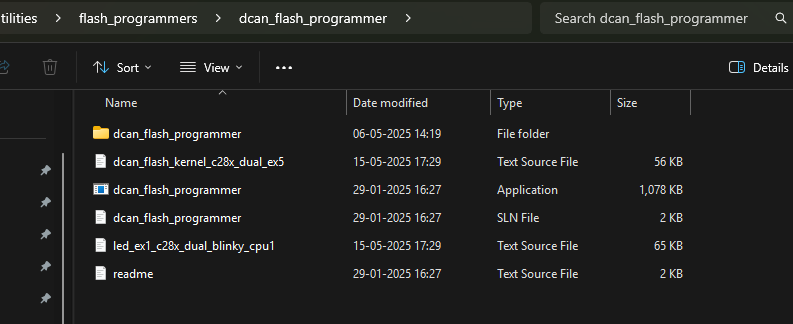
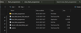
Flashing Command:C:\ti\C2000Ware_5_04_00_00\utilities\flash_programmers\dcan_flash_programmer>dcan_flash_programmer.exe -d f28p65x -k dcan_flash_kernel_c28x_dual_ex5.txt -a
The application seems to load successfully, as shown in the following console output: led_ex1_c28x_dual_blinky_cpu1.txt -v

Steps:
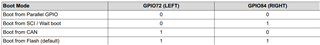
1.Set the boot mode to CAN: S3 with GPIO72 high and GPIO84 low.
2.loaded the -d f28p65x -k dcan_flash_kernel_c28x_dual_ex5.txt -a led_ex1_c28x_dual_blinky_cpu1.txt -v
3.after application loaded the GPIO72 Low and GPIO84 High, then Reset the Boad , but my application was not running.
Any guidance, example projects, or best practices would be highly appreciated.
Note:After resetting the board, the application does not run. The expected blinking behavior from led_ex1_c28x_dual_blinky_cpu1 is not observed.
Thank you in advance for your support.
Best regards,
Suresh k