Part Number: LAUNCHXL-F280039C
Other Parts Discussed in Thread: TIDM-DC-DC-BUCK, C2000WARE
Tool/software:
Hi everyone,
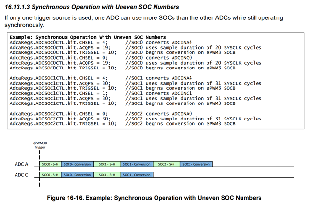
I'm developing code for one PWM (PWM1) to trigger multiple ADCs.
1. My main issue is that the GPIO 20 interrupt frequency differs from the PWM switching frequency.
I need assistance resolving this discrepancy.
2. I require the PWM to operate in up-count mode.
(Additionally, I not sure that my PWM settings are correct, specifically aiming for either CMPA at max duty and CMPB at zero duty, or vice-versa.)
The code:
//
// Included Files
//
#include "f28x_project.h"
#include "stdio.h"
#include "math.h"
// Defines
#define RESULTS_BUFFER_SIZE 256
//
// Globals
//
uint16_t adcAResults[RESULTS_BUFFER_SIZE]; // Buffer for results
uint16_t index; // Index into result buffer
volatile uint16_t bufferFull; // Flag to indicate buffer is full
// ADC pins for detecting analog values (digital)
unsigned int ADC_A6;
unsigned int ADC_B6;
unsigned int ADC_C0;
unsigned int ADC_A3_1;
unsigned int ADC_A3_2;
unsigned int ADC_B14_1;
unsigned int ADC_B14_2;
// Values for digital turning back to analog (analog)
float VAC_N_A6; // ADC_A6_Voltage_N
float VAC_L_B6; // ADC_B6_Voltage_L
float VO_C0; // ADC_C0_Voltage_Out
float IL_A3_1; // ADC_A3_Current_Sense
float IL_A3_2; // ADC_A3_Current_Sense
float IL_Ref_B14_1; // ADC_B14_Current_Ref
float IL_Ref_B14_2; // ADC_B14_Current_Ref
//
// Function Prototypes
void initEPWM(void);
void initADC(void);
void initADCSOC(void);
__interrupt void adcA1ISR(void);
//
// Main
//
void main(void)
{
// Initialize device clock and peripherals
InitSysCtrl();
// Initialize GPIO
InitGpio();
EALLOW;
/// GPIO20: It is for checking the ADC interrupt is working properly or not
GpioCtrlRegs.GPAPUD.bit.GPIO20 = 0; // Disable pull-up res. on GPIO20
GpioCtrlRegs.GPAMUX2.bit.GPIO20 = 0; // Configure GPIO20 as a GPIO pin
GpioCtrlRegs.GPADIR.bit.GPIO20 = 1; // Configure GPIO20 direction
EDIS;
// Disable CPU interrupts
DINT;
//
// Initialize the PIE control registers to their default state.
// The default state is all PIE interrupts disabled and flags
// are cleared.
//
InitPieCtrl();
//
// Disable CPU interrupts and clear all CPU interrupt flags:
//
IER = 0x0000;
IFR = 0x0000;
//
// Initialize the PIE vector table with pointers to the shell Interrupt
// Service Routines (ISR).
//
InitPieVectTable();
// Map ISR functions
EALLOW;
PieVectTable.ADCA1_INT = &adcA1ISR; // Function for ADCA interrupt 1
EDIS;
// Configure the ePWM
initEPWM();
// Configure the ADC and power it up
initADC();
// Setup the ADC for ePWM triggered conversions on channel 1
initADCSOC();
// Enable global Interrupts and higher priority real-time debug events:
//
IER |= M_INT1; // Enable group 1 interrupts
EINT; // Enable Global interrupt INTM
ERTM; // Enable Global realtime interrupt DBGM
//
// Initialize results buffer
//
for(index = 0; index < RESULTS_BUFFER_SIZE; index++)
{
adcAResults[index] = 0;
}
index = 0;
bufferFull = 0;
//
// Enable PIE interrupt
//
PieCtrlRegs.PIEIER1.bit.INTx1 = 1;
//
// Sync ePWM
//
EALLOW;
CpuSysRegs.PCLKCR0.bit.TBCLKSYNC = 1;
EDIS;
//
// Take conversions indefinitely in loop
//
while(1) {
}
}
//
// adcA1ISR - ADC A Interrupt 1 ISR
//
__interrupt void adcA1ISR(void){
GpioDataRegs.GPASET.bit.GPIO20 = 1;
// For reading the ADC values of A6 & B6 &C0 pins of SOC0...
// and B14 & A11 pins of SOC1. SOC2. SOC3
ADC_A6 = AdcaResultRegs.ADCRESULT0; // ADC of VAC_N
ADC_B6 = AdcbResultRegs.ADCRESULT0; // ADC of VAC_L
ADC_C0 = AdccResultRegs.ADCRESULT0; // ADC of Vout
ADC_A3_1 = AdcaResultRegs.ADCRESULT1; // ADC of IL
ADC_A3_2 = AdcaResultRegs.ADCRESULT2;
ADC_B14_1 = AdcbResultRegs.ADCRESULT1; // ADC of IL_Ref (1.65V)
ADC_B14_2 = AdcbResultRegs.ADCRESULT2;
// For converting the ADC values from digital to analog...
// of A6 & B6 & C0 and A3(oversamplings) & B14(oversamplings)
VAC_N_A6 = (float)(ADC_A6/4095.0)*3.3;
VAC_L_B6 = (float)(ADC_B6/4095.0)*3.3;
VO_C0 = (float)(ADC_C0/4095.0)*3.3;
IL_A3_1 = (float)(ADC_A3_1/4095.0)*3.3;
IL_A3_2 = (float)(ADC_A3_2/4095.0)*3.3;
IL_Ref_B14_1 = (float)(ADC_B14_1/4095.0)*3.3;
IL_Ref_B14_2 = (float)(ADC_B14_2/4095.0)*3.3;
GpioDataRegs.GPACLEAR.bit.GPIO20 = 1;
AdcaRegs.ADCINTFLGCLR.bit.ADCINT1 = 1; //clear INT1 flag
if(1 == AdcaRegs.ADCINTOVF.bit.ADCINT1){
AdcaRegs.ADCINTOVFCLR.bit.ADCINT1 = 1; //clear INT1 overflow flag
AdcaRegs.ADCINTFLGCLR.bit.ADCINT1 = 1; //clear INT1 flag
}
PieCtrlRegs.PIEACK.all = PIEACK_GROUP1; // Acknowledge the interrupt
}
//
// initEPWM - Function to configure ePWM1 to generate the SOC.
//
void initEPWM(void)
{
EALLOW;
/// ---------------------------------------- EPWM1 ---------------------------------------- ///
// Setup GPIO ----------------------------------------------------------------------------- ///
GpioCtrlRegs.GPAPUD.bit.GPIO0=1; // Disable pull-up res. on GPIO0 (EPWM1A)
GpioCtrlRegs.GPAMUX1.bit.GPIO0=1; // Configure GPIO0 as EPWM1A
GpioCtrlRegs.GPAPUD.bit.GPIO1=1; // Disable pull-up res. on GPIO1 (EPWM1B)
GpioCtrlRegs.GPAMUX1.bit.GPIO1=1; // Configure GPIO1 as EPWM1B
// Event Trigger and Interrupt(ET) Submodule:
EPwm1Regs.ETSEL.bit.SOCAEN = 1; // Enable SOCA
EPwm1Regs.ETSEL.bit.SOCASEL = 2; // 001: Enable event time-base counter equal to zero
EPwm1Regs.ETPS.bit.SOCAPRD = 1; // Generate pulse on 1st event
// Setup Time-Base(TB) Submodule ---------------------------------------------------------- ///
// Config for the frequency and duty cycle of the EPWM1
EPwm1Regs.TBPRD = 1199; // Set period counts
EPwm1Regs.CMPA.bit.CMPA = 600; // Setup compare value
EPwm1Regs.CMPB.bit.CMPB = 1199; // Setup compare value
// Setup TBCLK
CpuSysRegs.PCLKCR0.bit.TBCLKSYNC = 1; // Set TBCLKSYNC = 1
CpuSysRegs.PCLKCR2.bit.EPWM1 = 1; // Enable ePWM module clocks in the PCLKCRx register
// TBCLK = EPWMCLK / (HSPCLKDIV * CLKDIV)
EPwm1Regs.TBCTL.bit.HSPCLKDIV = 0; // HSPCLKDIV = 1
EPwm1Regs.TBCTL.bit.CLKDIV = 0; // CLKDIV = 1
// Counter mode
EPwm1Regs.TBCTL.bit.CTRMODE = 0; // (0)Count up
// ePWM Phase setting
EPwm1Regs.TBCTL.bit.PHSEN = 0; // (0)Disable phase loading
EPwm1Regs.TBPHS.bit.TBPHS = 0; // Phase is 0
CpuSysRegs.PCLKCR0.bit.TBCLKSYNC = 0; // Set TBCLKSYNC = 0
EPwm1Regs.TBCTR = 0; // Time Base Counter Register
//EPwm1Regs.EPWMSYNCOUTEN.bit.ZEROEN = 1;
// Setup Counter-Compare(CC) Submodule ---------------------------------------------------- ///
EPwm1Regs.CMPCTL.bit.SHDWAMODE = 0; // Load registers every ZERO
EPwm1Regs.CMPCTL.bit.SHDWBMODE = 0;
EPwm1Regs.CMPCTL.bit.LOADAMODE = 0;
EPwm1Regs.CMPCTL.bit.LOADBMODE = 0;
// Setup Action-Qualifier(AQ) Submodule --------------------------------------------------- ///
EPwm1Regs.AQCTLA.bit.ZRO = 2; // Action when TBCTR = 0; 2: force EPWM1A output high.
EPwm1Regs.AQCTLA.bit.CAU = 1; // Action when TBCTR = CMPA on Up-count; 1: force EPWM1A output low.
EPwm1Regs.AQCTLB.bit.CAU = 1; // Action when TBCTR = CMPA on Up-count; 2: force EPWM1B output high.
EPwm1Regs.AQCTLB.bit.CBU = 2; // Action when TBCTR = CMPA on Up-count; 1: force EPWM1B output low.
// Setup Dead-Band(DB) Submodule --------------------------------------------------- ///
EPwm1Regs.DBCTL.bit.IN_MODE = 2;
EPwm1Regs.DBCTL.bit.POLSEL = 2; // EPWMxA directly output(D); EPWMxB inverted output(1-D)
EPwm1Regs.DBCTL.bit.OUT_MODE = 3; // Enable the deadtime.
EPwm1Regs.DBRED.bit.DBRED = 48; // 1u = DBRED * (1/120M) => DBRED = 120
EPwm1Regs.DBFED.bit.DBFED = 48; // 24 = 200n(= 10u*2% );40=345n;25=230n
EDIS;
}
//
// initADC - Function to configure and power up ADCA.
//
void initADC(void){
// Setup VREF as internal for ADC-A & ADC-B & ADC-C
SetVREF(ADC_ADCA, ADC_INTERNAL, ADC_VREF3P3);
SetVREF(ADC_ADCB, ADC_INTERNAL, ADC_VREF3P3);
SetVREF(ADC_ADCC, ADC_INTERNAL, ADC_VREF3P3);
EALLOW;
// ADC-A Group Settings
AdcaRegs.ADCCTL2.bit.PRESCALE = 6; // Set ADCCLK divider to /4
AdcaRegs.ADCCTL1.bit.INTPULSEPOS = 1; // Set pulse positions to late
AdcaRegs.ADCCTL1.bit.ADCPWDNZ = 1; // Power up the ADC and then delay for 1 ms
// ADC-B Group Settings
AdcbRegs.ADCCTL2.bit.PRESCALE = 6; // Set ADCCLK divider to /4
AdcbRegs.ADCCTL1.bit.INTPULSEPOS = 1; // Set pulse positions to late
AdcbRegs.ADCCTL1.bit.ADCPWDNZ = 1; // Power up the ADC and then delay for 1 ms
// ADC-C Group Settings
AdccRegs.ADCCTL2.bit.PRESCALE = 6; // Set ADCCLK divider to /4
AdccRegs.ADCCTL1.bit.INTPULSEPOS = 1; // Set pulse positions to late
AdccRegs.ADCCTL1.bit.ADCPWDNZ = 1; // Power up the ADC and then delay for 1 ms
EDIS;
DELAY_US(1000);
}
//
// initADCSOC - Function to configure ADCA's SOC0 to be triggered by ePWM1.
//
void initADCSOC(void){
EALLOW;
/// SOCs Configuration -------------------------------------------------------------------- ///
/// SOC* will convert pin A*. B*. C* // 0:A0 1:A1 2:A2 3:A3 4:A4 5:A5 6:A6 7:A7
// 8:A8 9:A9 A:A10 B:A11
// C:A12 D:A13 E:A14 F:A15
/// A6 & B6 & C0 Settings of SOC0
/// A6 - SOC0
AdcaRegs.ADCSOC0CTL.bit.CHSEL = 6; // SOC0 will convert pin A6
AdcaRegs.ADCSOC0CTL.bit.ACQPS = 19; // Sample window is 10 SYSCLK cycles
AdcaRegs.ADCSOC0CTL.bit.TRIGSEL = 5; // Trigger on ePWM1 SOCA
/// B6 - SOC0
AdcbRegs.ADCSOC0CTL.bit.CHSEL = 6; // SOC0 will convert pin B6
AdcbRegs.ADCSOC0CTL.bit.ACQPS = 19; // Sample window is 10 SYSCLK cycles
AdcbRegs.ADCSOC0CTL.bit.TRIGSEL = 5; // Trigger on ePWM1 SOCA
/// C0 - SOC0
AdccRegs.ADCSOC0CTL.bit.CHSEL = 0;
AdccRegs.ADCSOC0CTL.bit.ACQPS = 19; // Sample window is 10 SYSCLK cycles
AdccRegs.ADCSOC0CTL.bit.TRIGSEL = 5; // Trigger on ePWM1 SOCA
/// B14 Settings of SOC1. SOC2. SOC3 & A3 Settings of SOC1. SOC2. SOC3
/// A3 - SOC1.SOC2.SOC3
AdcaRegs.ADCSOC1CTL.bit.CHSEL = 3; // SOC1 will convert pin A3
AdcaRegs.ADCSOC1CTL.bit.ACQPS = 19; // Sample window is 10 SYSCLK cycles
AdcaRegs.ADCSOC1CTL.bit.TRIGSEL = 5;
AdcaRegs.ADCSOC2CTL.bit.CHSEL = 3; // SOC2 will convert pin A3
AdcaRegs.ADCSOC2CTL.bit.ACQPS = 19; // Sample window is 10 SYSCLK cycles
AdcaRegs.ADCSOC2CTL.bit.TRIGSEL = 5;
/// B14 - SOC1.SOC2.SOC3
AdcbRegs.ADCSOC1CTL.bit.CHSEL = 14; // SOC1 will convert pin B14
AdcbRegs.ADCSOC1CTL.bit.ACQPS = 19; // Sample window is 10 SYSCLK cycles
AdcbRegs.ADCSOC1CTL.bit.TRIGSEL = 5; // Trigger on ePWM1 SOC
AdcbRegs.ADCSOC2CTL.bit.CHSEL = 14; // SOC2 will convert pin B14
AdcbRegs.ADCSOC2CTL.bit.ACQPS = 19; // Sample window is 10 SYSCLK cycles
AdcbRegs.ADCSOC2CTL.bit.TRIGSEL = 5; // Trigger on ePWM1 SOCA
///The INT1 settings. "INT1SEL" must configure according to the end of the SOCs.(ex: this program is end of SOC1)
AdcaRegs.ADCINTSEL1N2.bit.INT1SEL = 0; // End of SOC1 will set INT1 flag
AdcaRegs.ADCINTSEL1N2.bit.INT1E = 1; // Enable INT1 flag
AdcaRegs.ADCINTFLGCLR.bit.ADCINT1 = 1; // Make sure INT1 flag is cleared
EDIS;
}