This thread has been locked.

If you have a related question, please click the "Ask a related question" button in the top right corner. The newly created question will be automatically linked to this question.

TMS320F28335: Power on issue

Part Number: TMS320F28335
Other Parts Discussed in Thread: TPS563200

Tool/software:

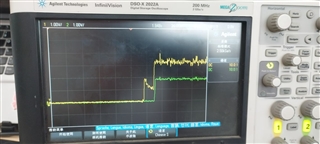
I am using TPS563200 to supply 1.9V and 3.3V power supplies such as IO to F28335 arch core power supply. The waveform of the power on is as follows: yellow is 3.3V, blue is 1.9V; sometimes the program can start normally, sometimes it cannot. Is it related to the power on sequence? Is the waveform abnormal? What other suggestions do you have regarding the issue of the program not starting properly? The same TPS563200, if not connected to F283353.3V output, is normal without the jitter shown in the figure;

  • Hi,

    I will need a few days to get back to you about this.

    Best Regards,

    Ben Collier

  • Hi,

    Please see the power sequencing section from the datasheet: 

    No requirements are placed on the power-up and power-down sequences of the various power pins to ensure the correct reset state for all the modules. However, if the 3.3-V transistors in the level shifting output buffers of the I/O pins are powered prior to the 1.9-V/1.8-V transistors, it is possible for the output buffers to turn on, causing a glitch to occur on the pin during power up. To avoid this behavior, power the VDD (core voltage) pins prior to or simultaneously with the VDDIO (input/output voltage) pins, ensuring that the VDD pins have reached 0.7 V before or at the same time as the VDDIO pins reach 0.7 V. There are some requirements on the XRS pin: 1. During power up, the XRS pin must be held low for tw(RSL1) after the input clock is stable (see Section 7.9.2.2). This is to enable the entire device to start from a known condition. 2. During power down, the XRS pin must be pulled low at least 8 μs prior to VDD reaching 1.5 V. Meeting this requirement is important to help prevent unintended flash program or erase. No voltage larger than a diode drop (0.7 V) above VDDIO should be applied to any digital pin (for analog pins, this value is 0.7 V above VDDA) before powering up the device. Furthermore, VDDIO and VDDA should always be within 0.3 V of each other. Voltages applied to pins on an unpowered device can bias internal P-N junctions in unintended ways and produce unpredictable results.

    You should power VDD before VDDIO.

    Best Regards,

    Ben Collier