Part Number: TMS320F280049
Other Parts Discussed in Thread: C2000WARE
Tool/software:
Hi experts
Abnormality Description:
The module fails to operate normally, with a defect rate of 1 piece per 100 pieces.
Analysis Process:
1. Visual inspection revealed no issues.
2. The chip was reprogrammed successfully.
3. Peripheral circuit analog signals and supply voltages were tested, with no abnormalities found.
The following signals were tested and confirmed normal:
① PIN22 (Iout+): ~1.55V (normal)
② PIN8 (VCCSEN): ~1.69V (normal)
③ PIN6 (VIN_S): ~1.44V (normal)
④ PIN23 (VTEMP): ~2.99V (normal)
⑤ PIN16 (VO_S) and PIN21 (ADC_A4): ~0V (normal)
⑥ PIN20 (S_3V3): ~3.3V (normal)
4. Software Engineer Aiden found incorrect clock timing during program testing.
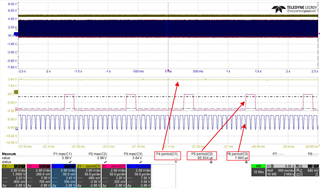
① First Test
GPIO Configuration Test:
Pin-4-XRSN: stable high level; Pin-31-GPIO17 pulse period: 100μs; Pin36-GPIO35 pulse period: 8μs
Test Results:
In normal modules, pulse periods matched the defined values. In faulty modules, the pulse periods were: Pin-31-GPIO17: 1000μs; Pin36-GPIO35: 80μs. All periods in faulty modules were longer than normal, and the watchdog kept resetting.
As shown below:
Normal Module
C1 (yellow: reset signal XRSN), C2 (red: GPIO17), C3 (blue: GPIO35)
Abnormal Module
C1 (yellow: reset signal XRSN), C2 (red: GPIO17), C3 (blue: GPIO35)
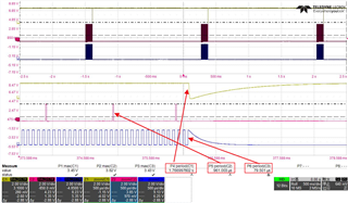
② Second Test
To identify patterns, the pulse periods in the test program were doubled, and differences between normal and abnormal modules were compared.
GPIO Configuration Test:
Pin-4-XRSN: stable high level; Pin-31-GPIO17 pulse period: 200μs; Pin36-GPIO35 pulse period: 16μs
Test Results:
In normal modules, pulse periods matched the defined values. In faulty modules, the pulse periods remained: Pin-31-GPIO17: 1000μs; Pin36-GPIO35: 80μs. The periods in faulty modules did not change, and the watchdog kept resetting.
As shown below:
Normal Module
C1 (yellow: reset signal XRSN), C2 (red: GPIO17), C3 (blue: GPIO35)
Abnormal Module
C1 (yellow: reset signal XRSN), C2 (red: GPIO17), C3 (blue: GPIO35)
5. The internal clock configuration resistor R435 was checked. Its resistance value was normal (1KΩ), and the connection was secure with no cold soldering.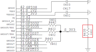
Summary:
1. For the faulty MCU: After reflow soldering, the 3.3V power supply was normal, and the internal clock configuration resistor R435 (1KΩ) was functional. The test program could be burned successfully, but the I/O port pulse periods did not match the programmed settings. When the programmed periods were doubled, the I/O port periods remained unchanged and still did not match the settings.
2. Replacing the MCU restored normal module performance, while reinstalling the original MCU reproduced the abnormality. This indicates no issues with peripheral circuits and confirms the MCU itself has a functional abnormality.
Based on the previous report, additional experiments were conducted. The internal clocks (INTOSC1 and INTOSC2) and the phase-locked loop (PLL) system clock output (PLLSYSCLK) were output via GPIO. An oscilloscope measured the frequency of both INTOSC1 and INTOSC2 at 10 MHz, and the PLLSYSCLK frequency also remained at 10 MHz. After modifying the PLL's frequency multiplication and division configuration parameters, the PLLSYSCLK frequency still stayed at 10 MHz unchanged.
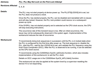
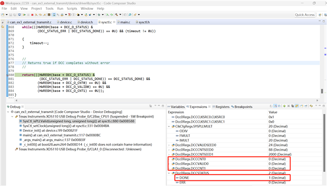
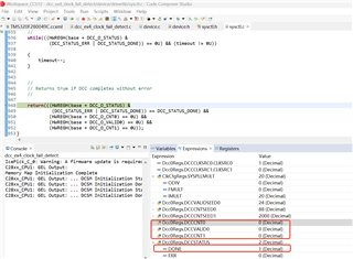
This afternoon, further problem localization testing revealed that during clock initialization in the faulty module, the PLL validity check feedback consistently indicated failure. Please assist in identifying under what circumstances this issue may occur.