Part Number: TMS320F28069
Tool/software:
The chip functions properly when debugged using the XDS100V2 emulator. The LCD control function within the RTOS task executes successfully, but the LCD exhibits flickering.When the XDS100V2 emulator is used for power supply without debugging, the LCD light control function in the RTOS task fails to run, and the LCD light does not light up.
Here's my CMD code::./*
//###########################################################################
//
// FILE: F28067.cmd
//
// TITLE: Linker Command File For F28067 Device
//
//###########################################################################
// $TI Release: F2806x C/C++ Header Files and Peripheral Examples V135 $
// $Release Date: Sep 8, 2012 $
//###########################################################################
*/
/* ======================================================
// For Code Composer Studio V2.2 and later
// ---------------------------------------
// In addition to this memory linker command file,
// add the header linker command file directly to the project.
// The header linker command file is required to link the
// peripheral structures to the proper locations within
// the memory map.
//
// The header linker files are found in <base>\F2806x_headers\cmd
//
// For BIOS applications add: F2806x_Headers_BIOS.cmd
// For nonBIOS applications add: F2806x_Headers_nonBIOS.cmd
========================================================= */
/* ======================================================
// For Code Composer Studio prior to V2.2
// --------------------------------------
// 1) Use one of the following -l statements to include the
// header linker command file in the project. The header linker
// file is required to link the peripheral structures to the proper
// locations within the memory map */
/* Uncomment this line to include file only for non-BIOS applications */
/* -l F2806x_Headers_nonBIOS.cmd */
/* Uncomment this line to include file only for BIOS applications */
/* -l F2806x_Headers_BIOS.cmd */
/* 2) In your project add the path to <base>\F2806x_headers\cmd to the
library search path under project->build options, linker tab,
library search path (-i).
/*========================================================= */
/* Define the memory block start/length for the F2806x
PAGE 0 will be used to organize program sections
PAGE 1 will be used to organize data sections
Notes:
Memory blocks on F28067 are uniform (ie same
physical memory) in both PAGE 0 and PAGE 1.
That is the same memory region should not be
defined for both PAGE 0 and PAGE 1.
Doing so will result in corruption of program
and/or data.
Contiguous SARAM memory blocks can be combined
if required to create a larger memory block.
*/
// The user must define CLA_C in the project linker settings if using the
// CLA C compiler
// Project Properties -> C2000 Linker -> Advanced Options -> Command File
// Preprocessing -> --define
#ifdef CLA_C
// Define a size for the CLA scratchpad area that will be used
// by the CLA compiler for local symbols and temps
// Also force references to the special symbols that mark the
// scratchpad are.
_Cla1Prog_Start = _Cla1funcsRunStart;
CLA_SCRATCHPAD_SIZE = 0x100;
--undef_sym=__cla_scratchpad_end
--undef_sym=__cla_scratchpad_start
#endif //CLA_C
MEMORY
{
PAGE 0 : /* Program Memory */
/* Memory (RAM/FLASH/OTP) blocks can be moved to PAGE1 for data allocation */
RAMM1 : origin = 0x000400, length = 0x000400 /* on-chip RAM block M1 */
RAML3 : origin = 0x009000, length = 0x001000
RAML45 : origin = 0x00A000, length = 0x003000
/*RAML0 : origin = 0x008000, length = 0x000800 on-chip RAM block L0 */
/*RAML1 : origin = 0x008800, length = 0x000400 on-chip RAM block L1 */
/*RAML2 : origin = 0x008C00, length = 0x000400 on-chip RAM block L2 */
/*RAML3 : origin = 0x009000, length = 0x001000 on-chip RAM block L2 */
/*RAML4 : origin = 0x00A000, length = 0x002000 on-chip RAM block L4 */
OTP : origin = 0x3D7800, length = 0x000400 /* on-chip OTP */
/*FLASHH : origin = 0x3D8000, length = 0x004000 on-chip FLASH */
/*FLASHG : origin = 0x3DC000, length = 0x004000 on-chip FLASH */
/*FLASHF : origin = 0x3E0000, length = 0x004000 on-chip FLASH */
/* FLASHEND : origin = 0x3E4000, length = 0x000100*/
/* FLASHEND : origin = 0x3E4000, length = 0x000020*/
/*FLASHTYPE : origin = 0x3E4020, length = 0x0000E0*/
FLASHJClr1 : origin = 0x3D8100, length = 0x000100
FLASHJClr2 : origin = 0x3D8200, length = 0x000100
FLASHBCDEFG : origin = 0x3D8348, length = 0x01BCB4 /* on-chip FLASH */
DSPVISION : origin = 0x3D8300, length = 0x4
GOTOMAIN : origin = 0x3D8304, length = 0x4 /* on-chip FLASH */
FLASHEND : origin = 0x3D8308, length = 0x000020
FLASHTYPE : origin = 0x3D8328, length = 0x000020
/*FLASHSTART : origin = 0x3F3FFF, length = 0x01*/
DSP_BOOT : origin = 0x3F5000, length = 0x04 /* on-chip FLASH */
FLASHA : origin = 0x3F5004, length = 0x002F78 /* on-chip FLASH */
FLASH_BOOT : origin = 0x3F3FFC, length = 0x4 /* on-chip FLASH */
CSM_RSVD : origin = 0x3F7F80, length = 0x000076 /* Part of FLASHA. Program with all 0x0000 when CSM is in use. */
BEGIN : origin = 0x3F7FF6, length = 0x000002 /* Part of FLASHA. Used for "boot to Flash" bootloader mode. */
CSM_PWL_P0 : origin = 0x3F7FF8, length = 0x000008 /* Part of FLASHA. CSM password locations in FLASHA */
FPUTABLES : origin = 0x3FD860, length = 0x0006A0 /* FPU Tables in Boot ROM */
IQTABLES : origin = 0x3FDF00, length = 0x000B50 /* IQ Math Tables in Boot ROM */
IQTABLES2 : origin = 0x3FEA50, length = 0x00008C /* IQ Math Tables in Boot ROM */
IQTABLES3 : origin = 0x3FEADC, length = 0x0000AA /* IQ Math Tables in Boot ROM */
ROM : origin = 0x3FF3B0, length = 0x000C10 /* Boot ROM */
RESET : origin = 0x3FFFC0, length = 0x000002 /* part of boot ROM */
VECTORS : origin = 0x3FFFC2, length = 0x00003E /* part of boot ROM */
PAGE 1 : /* Data Memory */
/* Memory (RAM/FLASH/OTP) blocks can be moved to PAGE0 for program allocation */
/* Registers remain on PAGE1 */
BOOT_RSVD : origin = 0x000000, length = 0x000050 /* Part of M0, BOOT rom will use this for stack */
RAMM0 : origin = 0x000050, length = 0x0003B0 /* on-chip RAM block M0 */
RAMM012 : origin = 0x008000, length = 0x001000
/*CLARAM0 : origin = 0x008800, length = 0x000400 on-chip RAM block L0 */
/*CLARAM1 : origin = 0x008C00, length = 0x000400 on-chip RAM block L1 */
/*CLARAM2 : origin = 0x008000, length = 0x000800 on-chip RAM block L2 */
RAML5 : origin = 0x00D000, length = 0x001000
RAML678 : origin = 0x00E000, length = 0x006000
//RAML5678 : origin = 0x00D000, length = 0x007000
/*RAML5 : origin = 0x00C000, length = 0x002000 on-chip RAM block L5 */
/*RAML6 : origin = 0x00E000, length = 0x002000 on-chip RAM block L6 */
/*RAML7 : origin = 0x010000, length = 0x002000 on-chip RAM block L7 */
/*RAML8 : origin = 0x012000, length = 0x002000 on-chip RAM block L8 */
USB_RAM : origin = 0x040000, length = 0x000800 /* USB RAM */
CLA1_MSGRAMLOW : origin = 0x001480, length = 0x000080
CLA1_MSGRAMHIGH : origin = 0x001500, length = 0x000080
}
/* Allocate sections to memory blocks.
Note:
codestart user defined section in DSP28_CodeStartBranch.asm used to redirect code
execution when booting to flash
.TI.ramfunc user defined section to store functions that will be copied from Flash into RAM
*/
SECTIONS
{
/* Allocate program areas: */
.cinit : > FLASHBCDEFG, PAGE = 0
.pinit : > FLASHBCDEFG, PAGE = 0
.text : > FLASHBCDEFG, PAGE = 0
codestart : > BEGIN, PAGE = 0
.textJMP1 : > FLASHJClr1 PAGE = 0
.textJMP2 : > FLASHJClr2 PAGE = 0
codeupdate : > FLASHA, PAGE = 0 /* Added by Leon on Nov. 17, 2006 */
dspboot : > DSP_BOOT, PAGE = 0
GotoMain : > GOTOMAIN, PAGE = 0
BOOTFLAG : > FLASH_BOOT, PAGE = 0 //
DSPVision : > DSPVISION, PAGE = 0
/*FlashStart : > FLASHSTART PAGE = 0*/ /* Added by Leon on Nov. 17, 2006 */
FlashEnd : > FLASHEND PAGE = 0
FlashType : > FLASHTYPE PAGE = 0 /* added for Special flash flag for Main DSP */
BootRamfuncs : LOAD = FLASHA,
RUN = RAMM1,
LOAD_START(_Flash28_API_LoadStart),
LOAD_END(_Flash28_API_LoadEnd),
RUN_START(_Flash28_API_RunStart),
PAGE = 0
GROUP
{
ModuleCodeLib_RAM
ramfuncs
}
LOAD = FLASHBCDEFG,
RUN = RAML45,
LOAD_START(_RamfuncsLoadStart),
LOAD_SIZE(_RamfuncsLoadSize),
RUN_START(_RamfuncsRunStart),
PAGE = 0
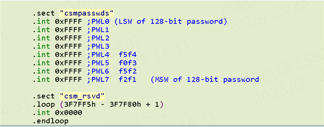
csmpasswds : > CSM_PWL_P0, PAGE = 0
csm_rsvd : > CSM_RSVD, PAGE = 0
/* Allocate uninitalized data sections: */
.stack : > RAML5, PAGE = 1
.ebss : > RAML678, PAGE = 1
.esysmem : > RAML678, PAGE = 1
OSStack : > RAML5, PAGE = 1
/* Initalized sections to go in Flash */
/* For SDFlash to program these, they must be allocated to page 0 */
.econst : > FLASHBCDEFG, PAGE = 0
.switch : > FLASHBCDEFG, PAGE = 0
/* Allocate IQ math areas: */
IQmath : > FLASHBCDEFG, PAGE = 0 /* Math Code */
IQmathTables : > IQTABLES, PAGE = 0, TYPE = NOLOAD
/* Allocate FPU math areas: */
FPUmathTables : > FPUTABLES, PAGE = 0, TYPE = NOLOAD
Cla1Prog : LOAD = FLASHBCDEFG,
RUN = RAML3,
LOAD_START(_Cla1funcsLoadStart),
LOAD_END(_Cla1funcsLoadEnd),
LOAD_SIZE(_Cla1funcsLoadSize),
RUN_START(_Cla1funcsRunStart),
PAGE = 0
CLADataRAM : > RAMM012, PAGE=1
Cla1ToCpuMsgRAM : > CLA1_MSGRAMLOW, PAGE = 1
CpuToCla1MsgRAM : > CLA1_MSGRAMHIGH, PAGE = 1
#ifdef CLA_C
/* CLA C compiler sections */
//
// Must be allocated to memory the CLA has write access to
//
CLAscratch :
{ *.obj(CLAscratch)
. += CLA_SCRATCHPAD_SIZE;
*.obj(CLAscratch_end) } > RAMM012, PAGE = 1
.scratchpad : > RAMM012, PAGE = 1
.bss_cla : > RAMM012, PAGE = 1
.const_cla : LOAD = FLASHBCDEFG,
RUN = RAMM012,
RUN_START(_Cla1ConstRunStart),
LOAD_START(_Cla1ConstLoadStart),
LOAD_SIZE(_Cla1ConstLoadSize),
PAGE = 1
#endif //CLA_C
ConstantsInRAM : > RAML678, PAGE = 1
DMARAML8 : > RAML678, PAGE = 1
/* Uncomment the section below if calling the IQNexp() or IQexp()
functions from the IQMath.lib library in order to utilize the
relevant IQ Math table in Boot ROM (This saves space and Boot ROM
is 1 wait-state). If this section is not uncommented, IQmathTables2
will be loaded into other memory (SARAM, Flash, etc.) and will take
up space, but 0 wait-state is possible.
*/
/*
IQmathTables2 : > IQTABLES2, PAGE = 0, TYPE = NOLOAD
{
IQmath.lib<IQNexpTable.obj> (IQmathTablesRam)
}
*/
/* Uncomment the section below if calling the IQNasin() or IQasin()
functions from the IQMath.lib library in order to utilize the
relevant IQ Math table in Boot ROM (This saves space and Boot ROM
is 1 wait-state). If this section is not uncommented, IQmathTables2
will be loaded into other memory (SARAM, Flash, etc.) and will take
up space, but 0 wait-state is possible.
*/
/*
IQmathTables3 : > IQTABLES3, PAGE = 0, TYPE = NOLOAD
{
IQmath.lib<IQNasinTable.obj> (IQmathTablesRam)
}
*/
/* .reset is a standard section used by the compiler. It contains the */
/* the address of the start of _c_int00 for C Code. /*
/* When using the boot ROM this section and the CPU vector */
/* table is not needed. Thus the default type is set here to */
/* DSECT */
.reset : > RESET, PAGE = 0, TYPE = DSECT
vectors : > VECTORS, PAGE = 0, TYPE = DSECT
}
/*
/*
//===========================================================================
// End of file.
//===========================================================================
*/
The abovementioned issue occurs after adding the following code.#pragma CODE_SECTION(ZeroCrossingInterrupt,"ramfuncs");
interrupt void ZeroCrossingInterrupt(void)
{
Uint32 dwZeroTemp;
dwZeroTemp = ECap1Regs.CAP1;
udwOPFrecyIntr = dwZeroTemp - udwLineZeroCrossingOld;
if(1 == ECap1Regs.ECFLG.bit.CEVT1)
{
udwLineZeroCrossingOld = dwZeroTemp;
}
ECap1Regs.ECCLR.bit.CTROVF = 1;
ECap1Regs.ECCLR.bit.INT = 1;
ECap1Regs.ECCLR.bit.CEVT1 = 1;
ECap1Regs.ECCTL2.bit.REARM = 1;
PieCtrlRegs.PIEACK.all = PIEACK_GROUP4;
}