


Part Number: LAUNCHXL-F28P65X
Other Parts Discussed in Thread: TMS320F28P659DK-Q1
Tool/software:
Hi team
My customer is using F28P65X for single stage OBC project. Pls help with the below questions they have during designing the main controller circuit of TMS320F28P659DK-Q1 (176Pins) based on TI’s development board “LAUNCHXL-F28P65X”
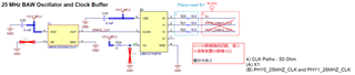
1. For the pin path from XTAL to DSP, there is a 50ohm impendence matching marked on schematics, but no 50ohm resistor is connected in series. So how to achieve the impendence matching?
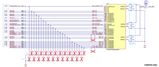
2. Regarding the MCU ADC ports, why the input capacitors are commented out? In the customer’s understanding, the input capacitors are used to provide filter function and provide transient current in high frequency sampling conditions, even need resistor in series to eliminate the oscillation.
3. Due to the special design in our project, customer put the MCU GND reference on HVDC- (high voltage DC output minus). Is it necessary to put an isolator between MCU side and JTAG input side? If yes, they need to generate additional 3.3V based on LV_GND for JTAG side and they also heard from their software engineer that the CCS may not be able to connect with their board with isolator (happens in the previous project). Could you please provide professional suggestions?
