This thread has been locked.

If you have a related question, please click the "Ask a related question" button in the top right corner. The newly created question will be automatically linked to this question.

TMS320F28P550SJ: The Large Inductance Current Causes the DSP to Reset

Part Number: TMS320F28P550SJ

Tool/software:

Hi experts

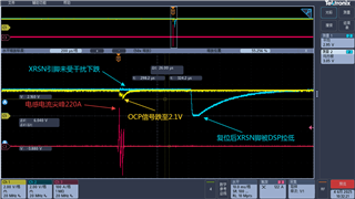
My customer is using 28P55 on their EV charging station power module. We found that The large inductance current causes the DSP to reset. The measured waveform shows that this disturbance does not affect the XRSN pin, does not trigger the TZ, and the 3.3V voltage on the VDD and VDDIO pins is also stable. The waveform is as follows:

CH1 represents that the OCP signal drops to 2.1V.

CH2 indicates that the XRSN signal does not drop due to interference during the inductor current spike, but after a while, the XRSN pin is pulled low.

CH3 represents the inductor current spike at 220A.

We attempted to locate the reset source. The reset cause readings from the RESC register showed it was an NMI reset. According to the NMISHDFLG register, the cause triggering the NMI is UNCERR (Uncorrectable Error). Later, we read the address 0x0000 0002 again, and the result was 0x0000 9A02. According to the table, this has nothing to do with the ECC (Error Correction Code) of either FLASH or CLA.

Please provide some suggestions to help troubleshoot the issue.

  • Hi Ehtan,

    What signals do the yellow (C1) and red (C3) traces represent?  Is there a waveform capture for the inductance current sensor that feeds to the ADC input?

    Thanks,

    Joseph

  • Sorry Ethan, I missed the notes above on what CH2 and CH3 represent.  I see that CH3 is the current sensor signal.  It is not clear though what the peak and minimum values are.  Anyway, the negative (minimum value) seems to be lower that -0.3V absolute input value.  This will cause not only XRSN issues but long term reliability issues as well if this condition happens too often.

    Would be good to introduce a clamping diode (TVS) or filters to prevent the inputs from going above the 3.3V rail and GND.  These instantaneous peak values may propagate to other blocks in the chip, especially the negative peak which appears to be exceeding the -0.3v absolute value and affect the operation of the MCU.

    Regards,

    Joseph