Other Parts Discussed in Thread: ADS1258
Tool/software:
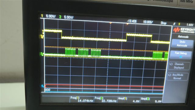
Hello,
I am working on the TMS320F28379D controller and I want to interface it with the ADS1258 via SPI. The main task is to read the default register values of the ADS1258. I have provided the code below, so please let me know what is wrong in it.
//###########################################################################
//
// FILE: Example_2837xDSpi_FFDLB.c
//
// TITLE: SPI Digital Loop Back program.
//
//! \addtogroup cpu01_example_list
//! <h1>SPI Digital Loop Back (spi_loopback)</h1>
//!
//! This program uses the internal loop back test mode of the peripheral.
//! Other then boot mode pin configuration, no other hardware configuration
//! is required. Interrupts are not used.
//!
//! A stream of data is sent and then compared to the received stream.
//! The sent data looks like this: \n
//! 0000 0001 0002 0003 0004 0005 0006 0007 .... FFFE FFFF \n
//! This pattern is repeated forever.
//!
//! \b Watch \b Variables \n
//! - \b sdata - sent data
//! - \b rdata - received data
//!
//
//###########################################################################
//
//
// $Copyright:
// Copyright (C) 2013-2024 Texas Instruments Incorporated - http://www.ti.com/
//
// Redistribution and use in source and binary forms, with or without
// modification, are permitted provided that the following conditions
// are met:
//
// Redistributions of source code must retain the above copyright
// notice, this list of conditions and the following disclaimer.
//
// Redistributions in binary form must reproduce the above copyright
// notice, this list of conditions and the following disclaimer in the
// documentation and/or other materials provided with the
// distribution.
//
// Neither the name of Texas Instruments Incorporated nor the names of
// its contributors may be used to endorse or promote products derived
// from this software without specific prior written permission.
//
// THIS SOFTWARE IS PROVIDED BY THE COPYRIGHT HOLDERS AND CONTRIBUTORS
// "AS IS" AND ANY EXPRESS OR IMPLIED WARRANTIES, INCLUDING, BUT NOT
// LIMITED TO, THE IMPLIED WARRANTIES OF MERCHANTABILITY AND FITNESS FOR
// A PARTICULAR PURPOSE ARE DISCLAIMED. IN NO EVENT SHALL THE COPYRIGHT
// OWNER OR CONTRIBUTORS BE LIABLE FOR ANY DIRECT, INDIRECT, INCIDENTAL,
// SPECIAL, EXEMPLARY, OR CONSEQUENTIAL DAMAGES (INCLUDING, BUT NOT
// LIMITED TO, PROCUREMENT OF SUBSTITUTE GOODS OR SERVICES; LOSS OF USE,
// DATA, OR PROFITS; OR BUSINESS INTERRUPTION) HOWEVER CAUSED AND ON ANY
// THEORY OF LIABILITY, WHETHER IN CONTRACT, STRICT LIABILITY, OR TORT
// (INCLUDING NEGLIGENCE OR OTHERWISE) ARISING IN ANY WAY OUT OF THE USE
// OF THIS SOFTWARE, EVEN IF ADVISED OF THE POSSIBILITY OF SUCH DAMAGE.
// $
//###########################################################################
//
// Included Files
//
#include "F28x_Project.h"
#include "ADS1258.h"
//
// Function Prototypes
//
void transmitData(uint16_t a);
void initSPIFIFO(void);
void error(void);
void InitSpi(void);
void InitSpiaGpio(void);
void InitADS1258Gpio(void);
void ADS1258_Reset(void);
void ADS1258_ReadRegisters(int start_addr, int num, int* buffer);
uint16_t spiTransfer(uint16_t data);
int i;
int regs[2];
int registerMap[NUM_REGISTERS];
void main(void)
{
// Step 1. Initialize System Control:
// PLL, WatchDog, enable Peripheral Clocks
// This example function is found in the F2837xD_SysCtrl.c file.
//
InitSysCtrl();
// Step 2. Initialize GPIO:
// This example function is found in the F2837xD_Gpio.c file and
// illustrates how to set the GPIO to it's default state.
// Setup only the GP I/O only for SPI-A functionality
// This function is found in F2837xD_Spi.c
//
InitSpiaGpio();
InitADS1258Gpio();
// Step 3. Clear all interrupts:
//
DINT;
// Initialize PIE control registers to their default state.
// The default state is all PIE __interrupts disabled and flags
// are cleared.
// This function is found in the F2837xD_PieCtrl.c file.
//
InitPieCtrl();
// Disable CPU __interrupts and clear all CPU __interrupt flags:
//
IER = 0x0000;
IFR = 0x0000;
// Initialize the PIE vector table with pointers to the shell Interrupt
// Service Routines (ISR).
// This will populate the entire table, even if the __interrupt
// is not used in this example. This is useful for debug purposes.
// The shell ISR routines are found in F2837xD_DefaultIsr.c.
// This function is found in F2837xD_PieVect.c.
//
InitPieVectTable();
//
// Step 4. Initialize the Device Peripherals:
//
spi_fifo_init(); // Initialize the SPI FIFO
adcStartupRoutine();
for(;;)
{
}
}
//
// delay_loop - Loop for a brief delay
//
void delay_loop()
{
long i;
for (i = 0; i < 1000000; i++) {}
}
//
// error - Error function that halts the debugger
//
void error(void)
{
asm(" ESTOP0"); // Test failed!! Stop!
for (;;);
}
//
// spi_xmit - Transmit value via SPI
//
void spi_xmit(Uint16 a)
{
SpiaRegs.SPITXBUF = a;
}
uint16_t spiTransfer(uint16_t data)
{
while(SpiaRegs.SPISTS.bit.BUFFULL_FLAG);
SpiaRegs.SPITXBUF = data;
while(SpiaRegs.SPISTS.bit.INT_FLAG == 0);
return SpiaRegs.SPIRXBUF;
}
//
// spi_fifo_init - Initialize SPIA FIFO
//
void spi_fifo_init()
{
//
// Initialize SPI FIFO registers
//
SpiaRegs.SPIFFTX.all = 0xE040;
SpiaRegs.SPIFFRX.all = 0x2044;
SpiaRegs.SPIFFCT.all = 0x0;
//
// Initialize core SPI registers
//
InitSpi();
}
void InitADS1258Gpio(void)
{
EALLOW;
GpioCtrlRegs.GPBMUX2.bit.GPIO52 = 0; // GPIO80 as GPIO
GpioCtrlRegs.GPBDIR.bit.GPIO52 = 1; // Output (PWDN)
GpioCtrlRegs.GPDMUX1.bit.GPIO97 = 0; // GPIO84 as GPIO
GpioCtrlRegs.GPDDIR.bit.GPIO97 = 1; // Output (RESET)
GpioCtrlRegs.GPCMUX1.bit.GPIO67 = 0; // GPIO4 as GPIO
GpioCtrlRegs.GPCDIR.bit.GPIO67 = 1; // Output (START)
EDIS;
}
void adcStartupRoutine(void)
{
/* (OPTIONAL) Provide additional delay time for power supply settling */
DELAY_US(50000); //5ms
/* (REQUIRED) Set nRESET/nPWDN pin high for ADC operation */
GpioDataRegs.GPBCLEAR.bit.GPIO52 = 1;
/* (OPTIONAL) Start ADC conversions with HW pin control */
GpioDataRegs.GPCCLEAR.bit.GPIO67 = 1;
/* (REQUIRED) tWAKE delay */
DELAY_US(50000);
/* (OPTIONAL) Toggle nRESET pin to assure default register settings. */
/* NOTE: This also ensures that the device registers are unlocked. */
GpioDataRegs.GPDCLEAR.bit.GPIO97 = 1; // RESET low
DELAY_US(10);
GpioDataRegs.GPDSET.bit.GPIO97 = 1; // RESET high
DELAY_US(10);
/* Ensure internal register array is initialized */
// restoreRegisterDefaults();
/* (OPTIONAL) Configure initial device register settings here*/
// uint8_t initRegisterMap[NUM_REGISTERS];
// initRegisterMap[REG_ADDR_CONFIG0] = CONFIG0_DEFAULT;
// initRegisterMap[REG_ADDR_CONFIG1] = CONFIG1_DLY_64us | CONFIG1_DRATE_7813SPS;
// initRegisterMap[REG_ADDR_MUXSCH] = MUXSCH_DEFAULT;
// initRegisterMap[REG_ADDR_MUXDIF] = MUXDIF_DEFAULT;
// initRegisterMap[REG_ADDR_MUXSG0] = MUXSG0_DEFAULT;
// initRegisterMap[REG_ADDR_MUXSG1] = MUXSG1_DEFAULT;
// initRegisterMap[REG_ADDR_SYSRED] = SYSRED_DEFAULT;
// initRegisterMap[REG_ADDR_GPIOC] = GPIOC_DEFAULT;
// initRegisterMap[REG_ADDR_GPIOD] = GPIOD_DEFAULT;
// initRegisterMap[REG_ADDR_ID] = 0x00; // Read-only register
/* (OPTIONAL) Write to all (writable) registers */
//writeMultipleRegisters(REG_ADDR_CONFIG0, NUM_REGISTERS - 1, initRegisterMap);
/* (OPTIONAL) Read back all registers */
// readMultipleRegisters(REG_ADDR_CONFIG0, NUM_REGISTERS);
//
// Read first 2 registers (0x00 and 0x01)
//
ADS1258_ReadRegisters(0x00, 2, regs);
/* (OPTIONAL) Start ADC conversions with the SPI command.
* Not needed if the START pin has already been set HIGH.
*
* sendCommand(START_OPCODE);
*/
}
//void writeMultipleRegisters(uint8_t startAddress, uint8_t count, const uint8_t regData[])
//{
// /* Check that the register address and count are in range */
// assert(startAddress + count <= NUM_REGISTERS);
//
// /* Check that regData is not a NULL pointer */
// assert(regData);
//
//
// //
// // SPI communication
// //
//
// GpioDataRegs.GPBSET.bit.GPIO61 = 0;
//
// uint8_t dataTx = OPCODE_WREG | OPCODE_MUL_MASK | (startAddress & OPCODE_A_MASK);
// spiSendReceiveByte(dataTx);
//
// uint8_t i;
// for (i = startAddress; i < startAddress + count; i++)
// {
// // write register data bytes
// spiSendReceiveByte(regData[i]);
//
// /* Update register array */
// registerMap[i] = regData[i];
// }
//
// GpioDataRegs.GPBSET.bit.GPIO61 = 1;
//}
void readMultipleRegisters(int startAddress, int count)
{
/* Check that the register address and count are in range */
assert(startAddress + count <= NUM_REGISTERS);
//
// SPI communication
//
GpioDataRegs.GPBSET.bit.GPIO61 = 0;
int dataTx = OPCODE_RREG | OPCODE_MUL_MASK | (startAddress & OPCODE_A_MASK);
spiTransfer(dataTx);
int i;
for (i = startAddress; i < startAddress + count; i++)
{
// Read register data bytes
registerMap[i] = spiTransfer(0x00);
}
GpioDataRegs.GPBSET.bit.GPIO61 = 1;
}
//
// Read Registers from ADS1258
//
void ADS1258_ReadRegisters(int start_addr, int num, int* buffer)
{
spiTransfer(0x10 | (start_addr & 0x0F)); // READ REG command
spiTransfer(num - 1); // Number of registers - 1
for ( i = 0; i < num; i++)
{
buffer[i] = (int)spiTransfer(0x00); // Read register
}
GpioDataRegs.GPASET.bit.GPIO19 = 1; // CS high
}