This thread has been locked.

If you have a related question, please click the "Ask a related question" button in the top right corner. The newly created question will be automatically linked to this question.

TMS320F28377D: ADC sampling noise design suggestions

Part Number: TMS320F28377D

Tool/software:

Hi Expert 

Customer use our F28377 in the power distribution unit they see some issues with ADC sampling as the picture shown below:

the blue line / white line/ yellow line are the incorrect ADC sampling output, when the power board powered up.
You can see the drop and rise of those 3 lines are the same, it means the same interfere signal may coupled to to 3 channels.

the green / red/ purple lines do not couples the interfere. 

the hardware connection are below:

 blue line - AI13(x0.58)-ADCIND2 / white line - AI7(x0.14) - ADCINB4 / yellow line - AI10(x1.4) - ADCINC2 , typical input circuit:
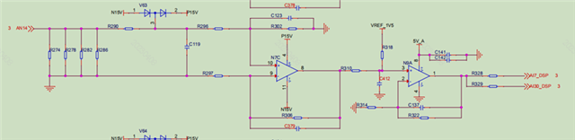
MCU schematic:

Do you have any suggestions to debug this issue?

Thanks

Joe

  • Hello,

    I will take a look and reply to you in timely manner.

  • Hi Stevan

    Kindly follow up this thread, Do you have any suggestions to debug this issue?

    Thanks

    Joe

  • Hello Joe,

    The ADC inputs should be kept below VDDA + 0.3 V during operation. If an ADC input exceeds this level, the VREF internal to the device may be disturbed, which can impact results for other ADC or DAC inputs using the same VREF.

    Also, the VREFHI pin must be kept below VDDA + 0.3 V to ensure proper functional operation. If the VREFHI pin exceeds this level, a blocking circuit may activate, and the internal value of VREFHI may float to 0 V internally, giving improper ADC conversion or DAC output.

  • Hi Stevan

    This issue does not looks like the over voltage issue, the reasons are below:

    if the ADC input channel input over voltage signal, the input signal should be first limited by the MCU internal TVS so the blue line / white line/ yellow line should at the maximum ADC value.

    if the VREFHI pin input voltage exceeds the VDDA + 0.3, all the ADC channels should appears the same issue, but now there is only several channels have this issue.

    I think one of the debug direction could be: Is there any possibility that MCU pin can couple the noise?

    Thanks

    Joe

  • Hi Joe,

    It would be good to measure your VDDA and VREFHI just as a sanity check. Have you checked if your RC values are properly configured and your set acquisition time is correct? You can check based on TI ADC model (Analog Engineers Calculator) or check the derivation of calculation in TRM.

  • Close this thread since no feedback from customer side.