


Part Number: TMS320F28P650DK
Tool/software:
Hi Champs,
I use F28P65 Launchpad and CCS12.8.1 for testing.
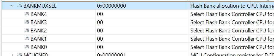
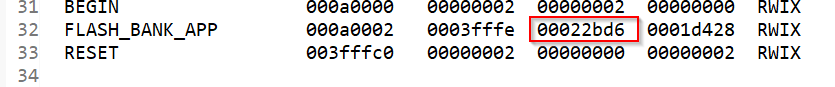
I defined flash bank 1 and 2 as FLASH_BANK_APP in .cmd file and used them. And in my code, I assigned all FLASH BANKs to CPU1.

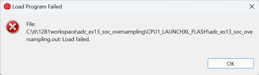
When the code size in my FLASH is less than 0x20000, my code is all stored in FLASH BANK1 and can be programmed normally. However, once the code size is greater than 0x20000, that is, the code needs to be stored in FLASH BANK1 and 2, my programming will fail and the error message is as follows:
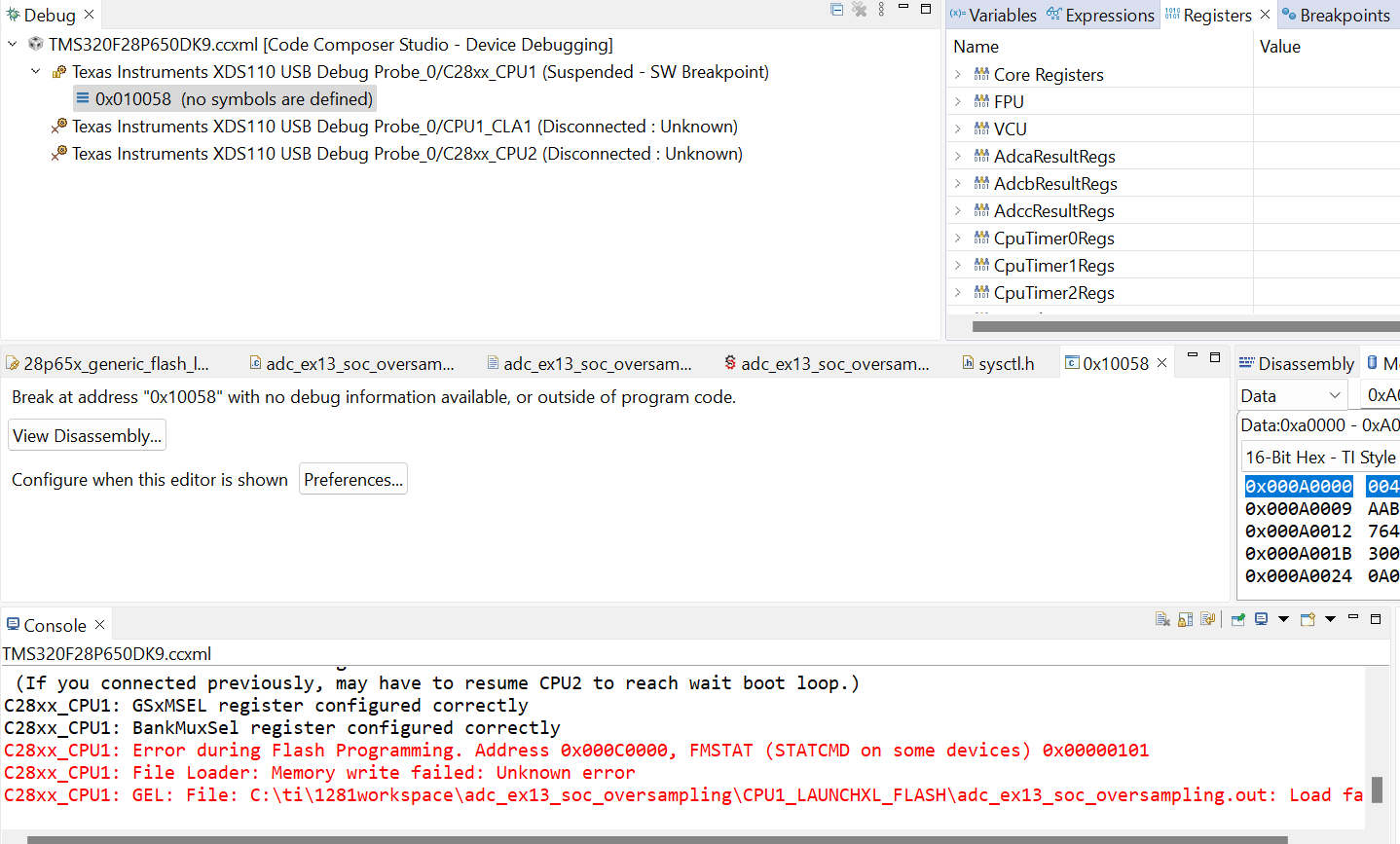
console window shows:
C28xx_CPU1: GEL Output:
Memory Map Initialization Complete
C28xx_CPU1: GEL Output: ... DCSM Initialization Start ...
C28xx_CPU1: GEL Output: ... DCSM Initialization Done ...
C28xx_CPU1: GEL Output:
 CPU2 is out of reset and configured to wait boot.
 (If you connected previously, may have to resume CPU2 to reach wait boot loop.)
C28xx_CPU1: If erase/program (E/P) operation is being done on one core, the other core should not execute from shared-RAM (SR) as they are used for the E/P code. User code execution from SR could commence after the selected flash banks are programmed.
C28xx_CPU1: Only CPU1 on-chip Flash Plugin can configure clock for CPU1, and CPU2 Flash operations. Plugin automatically configures PLL when CPU1 Flash operations are invoked. However, if users want to do only CPU2 Flash operations without doing a prior CPU1 operation in the current session, they should click on 'Configure Clock' button in CPU1's on-chip Flash Plugin before invoking CPU2 Flash operations. When this button is used, Flash Plugin will configure the clock for CPU1/CPU2 at 200MHz using INTOSC as the clock source. Plugin will leave PLL config like this and user application should configure the PLL as required by application.
C28xx_CPU1: Before doing any flash operations using the flash plugin, (a) Please select which flash banks should be mapped to which CPU (CPU1 vs CPU2) - This selection should be done in CPU1 flash plugin GUI. (b) Please select the flash banks that the user would like the flash plugin to erase (in the CPU1 flash plugin GUI and the CPU2 flash plugin GUI)
C28xx_CPU1: GEL Output: ... DCSM Initialization Start ...
C28xx_CPU1: GEL Output: ... DCSM Initialization Done ...
C28xx_CPU1: GEL Output:
 CPU2 is out of reset and configured to wait boot.
 (If you connected previously, may have to resume CPU2 to reach wait boot loop.)
C28xx_CPU1: GEL Output: ... DCSM Initialization Start ...
C28xx_CPU1: GEL Output: ... DCSM Initialization Done ...
C28xx_CPU1: GEL Output:
 CPU2 is out of reset and configured to wait boot.
 (If you connected previously, may have to resume CPU2 to reach wait boot loop.)
C28xx_CPU1: GEL Output: ... DCSM Initialization Start ...
C28xx_CPU1: GEL Output: ... DCSM Initialization Done ...
C28xx_CPU1: GEL Output:
 CPU2 is out of reset and configured to wait boot.
 (If you connected previously, may have to resume CPU2 to reach wait boot loop.)
C28xx_CPU1: GSxMSEL register configured correctly
C28xx_CPU1: BankMuxSel register configured correctly
C28xx_CPU1: Error during Flash Programming. Address 0x000C0000, FMSTAT (STATCMD on some devices) 0x00000101
C28xx_CPU1: File Loader: Memory write failed: Unknown error
C28xx_CPU1: GEL: File: C:\ti\1281workspace\adc_ex13_soc_oversampling\CPU1_LAUNCHXL_FLASH\adc_ex13_soc_oversampling.out: Load failed.
You can directly use my project below to reproduce this issue, I used a lot of duplicate code in my project, which increased the FLASH code size.
Thanks!
Best Regards,
Julia


