This thread has been locked.

If you have a related question, please click the "Ask a related question" button in the top right corner. The newly created question will be automatically linked to this question.

TMS320F28P650SK: GPIO status measurement after device power on

Part Number: TMS320F28P650SK

Tool/software:

Hi Champ, 

I am asking for my customer. 

They are using F28P650SK6PZPR (100-pin) device in their end equipment UPS. The device is on control card.

After device powers on and before user configures the IO pins to GPIO, during the time (circled in red) the IO pins are keeping as high-Z input. 
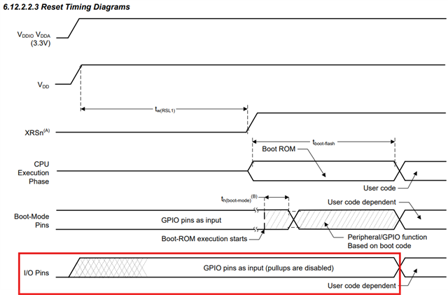
Customer encounters an issue that during the time (high-Z input), they measure the pin directly coming from MCU (disconnect the external circuit) that there is a voltage (~3.3V) big enough to cause the gate driver accidentally drive then damage the MOSFET. In the past, I have never seen a solid voltage coupling to the pin before. 

Remove control card from main board(eliminate system level), and capture the waveform on MCU pin directly.

CH1: Pin 99 

CH2: debug pin to know when the initialized GPIO configuration code is done 
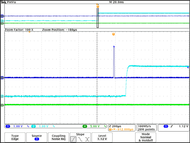
(1). Could the expert kindly check if the pin 99 in this package has any difference from other GPIOs ? or the voltage is caused by the GPIO input leakage current (I believe not) ? 

(2). Could team help to validate it on our 100-pin socket board with F28P650SK6PZPR and prove the device’s GPIO status during the time from device power on to user GPIO configuration ? It means a lot to prove the voltage not caused by the device.

Thanks for the support.

Regards,

Johnny

  • Hi expert,

    Any chance to have some input here.

    Thanks,

    Johnny

  • Hello,

    The GPIO/muxed pins default to GPIO‐input (high‐impedance) on reset / power‐on. High impedance means the pin is not actively driven (source or sink) by the MCU, so in principle it should float. Thus, the behavior you observe is not inherently impossible per the device‐spec; but getting ~3.3 V high enough to drive something suggests either there is an external circuit pulling it up, or direct internal clamping is involved. Is VDDIO / I/O supply coming up before or with the main chip? If some supplies are present, some internal circuits may be powered earlier, enabling bias or ESD clamp to act.

    Also, in some boot code or debug ROMs / startup sequences, pins might be configured or special code run before your GPIO init. Using a debug GPIO marker is good, but ensure no other early initialization touches it.

    Best Regards,

    Masoud

  • Hi Masoud,

    The GPIO/muxed pins default to GPIO‐input (high‐impedance) on reset / power‐on. High impedance means the pin is not actively driven (source or sink) by the MCU, so in principle it should float.

    I totally agree with you.

    However, I duplicate customer's issue with internal App's team 100-pin VDB (socket board).

    Indeed see the GPIO92 has a clear 3.3V during power on to user code dependent. 

    (1). Would you kindly test it with our 100-pin VDB as well ?

    (2). We trial and error, removing two pins' initialization in board_init(), and put those pins initialization code back in few lines later (attached code), then the 3.3V on GPIO92 was gone tested on 100-pin VDB.

    EPWM3 A (GPIO 4 / Pin 93)

    EPWM14 A (GPIO 203 / Pin 11)

    Board_init();
        GPIO_writePin(DEBUG_GPIO, 1);
        I2CFIFO_Init();
        LCD_Init();
        EALLOW;
        GPIO_setPinConfig(DD_EPWM_EPWMA_PIN_CONFIG);
        GPIO_setPadConfig(DD_EPWM_EPWMA_GPIO, GPIO_PIN_TYPE_STD);
        GPIO_setQualificationMode(DD_EPWM_EPWMA_GPIO, GPIO_QUAL_SYNC);
    
        GPIO_setPinConfig(DD_EPWM_EPWMB_PIN_CONFIG);
        GPIO_setPadConfig(DD_EPWM_EPWMB_GPIO, GPIO_PIN_TYPE_STD);
        GPIO_setQualificationMode(DD_EPWM_EPWMB_GPIO, GPIO_QUAL_SYNC);
        EPWM_setEmulationMode(DD_EPWM_BASE, EPWM_EMULATION_FREE_RUN);
        EPWM_setClockPrescaler(DD_EPWM_BASE, EPWM_CLOCK_DIVIDER_1, EPWM_HSCLOCK_DIVIDER_1);
        EPWM_setTimeBasePeriod(DD_EPWM_BASE, 999);
        EPWM_setTimeBaseCounter(DD_EPWM_BASE, 0);
        EPWM_setTimeBaseCounterMode(DD_EPWM_BASE, EPWM_COUNTER_MODE_UP);
        EPWM_disablePhaseShiftLoad(DD_EPWM_BASE);
        EPWM_setPhaseShift(DD_EPWM_BASE, 0);
        EPWM_setSyncInPulseSource(DD_EPWM_BASE, EPWM_SYNC_IN_PULSE_SRC_DISABLE);
        EPWM_setSyncPulseSource(DD_EPWM_BASE, HRPWM_PWMSYNC_SOURCE_ZERO);
        EPWM_setCounterCompareValue(DD_EPWM_BASE, EPWM_COUNTER_COMPARE_A, 0);
        EPWM_setCounterCompareShadowLoadMode(DD_EPWM_BASE, EPWM_COUNTER_COMPARE_A, EPWM_COMP_LOAD_ON_CNTR_ZERO);
        EPWM_setCounterCompareValue(DD_EPWM_BASE, EPWM_COUNTER_COMPARE_B, 0);
        EPWM_setCounterCompareShadowLoadMode(DD_EPWM_BASE, EPWM_COUNTER_COMPARE_B, EPWM_COMP_LOAD_ON_CNTR_ZERO);
        EPWM_setActionQualifierAction(DD_EPWM_BASE, EPWM_AQ_OUTPUT_A, EPWM_AQ_OUTPUT_HIGH, EPWM_AQ_OUTPUT_ON_TIMEBASE_ZERO);
        EPWM_setActionQualifierAction(DD_EPWM_BASE, EPWM_AQ_OUTPUT_A, EPWM_AQ_OUTPUT_NO_CHANGE, EPWM_AQ_OUTPUT_ON_TIMEBASE_PERIOD);
        EPWM_setActionQualifierAction(DD_EPWM_BASE, EPWM_AQ_OUTPUT_A, EPWM_AQ_OUTPUT_LOW, EPWM_AQ_OUTPUT_ON_TIMEBASE_UP_CMPA);
        EPWM_setActionQualifierAction(DD_EPWM_BASE, EPWM_AQ_OUTPUT_A, EPWM_AQ_OUTPUT_NO_CHANGE, EPWM_AQ_OUTPUT_ON_TIMEBASE_DOWN_CMPA);
        EPWM_setActionQualifierAction(DD_EPWM_BASE, EPWM_AQ_OUTPUT_A, EPWM_AQ_OUTPUT_NO_CHANGE, EPWM_AQ_OUTPUT_ON_TIMEBASE_UP_CMPB);
        EPWM_setActionQualifierAction(DD_EPWM_BASE, EPWM_AQ_OUTPUT_A, EPWM_AQ_OUTPUT_NO_CHANGE, EPWM_AQ_OUTPUT_ON_TIMEBASE_DOWN_CMPB);
        EPWM_setActionQualifierAction(DD_EPWM_BASE, EPWM_AQ_OUTPUT_B, EPWM_AQ_OUTPUT_HIGH, EPWM_AQ_OUTPUT_ON_TIMEBASE_ZERO);
        EPWM_setActionQualifierAction(DD_EPWM_BASE, EPWM_AQ_OUTPUT_B, EPWM_AQ_OUTPUT_NO_CHANGE, EPWM_AQ_OUTPUT_ON_TIMEBASE_PERIOD);
        EPWM_setActionQualifierAction(DD_EPWM_BASE, EPWM_AQ_OUTPUT_B, EPWM_AQ_OUTPUT_NO_CHANGE, EPWM_AQ_OUTPUT_ON_TIMEBASE_UP_CMPA);
        EPWM_setActionQualifierAction(DD_EPWM_BASE, EPWM_AQ_OUTPUT_B, EPWM_AQ_OUTPUT_NO_CHANGE, EPWM_AQ_OUTPUT_ON_TIMEBASE_DOWN_CMPA);
        EPWM_setActionQualifierAction(DD_EPWM_BASE, EPWM_AQ_OUTPUT_B, EPWM_AQ_OUTPUT_LOW, EPWM_AQ_OUTPUT_ON_TIMEBASE_UP_CMPB);
        EPWM_setActionQualifierAction(DD_EPWM_BASE, EPWM_AQ_OUTPUT_B, EPWM_AQ_OUTPUT_NO_CHANGE, EPWM_AQ_OUTPUT_ON_TIMEBASE_DOWN_CMPB);
        EPWM_setRisingEdgeDelayCountShadowLoadMode(DD_EPWM_BASE, EPWM_RED_LOAD_ON_CNTR_ZERO);
        EPWM_disableRisingEdgeDelayCountShadowLoadMode(DD_EPWM_BASE);
        EPWM_setFallingEdgeDelayCountShadowLoadMode(DD_EPWM_BASE, EPWM_FED_LOAD_ON_CNTR_ZERO);
        EPWM_disableFallingEdgeDelayCountShadowLoadMode(DD_EPWM_BASE);
        EPWM_setTripZoneAction(DD_EPWM_BASE, EPWM_TZ_ACTION_EVENT_TZA, EPWM_TZ_ACTION_LOW);
        EPWM_setTripZoneAction(DD_EPWM_BASE, EPWM_TZ_ACTION_EVENT_TZB, EPWM_TZ_ACTION_LOW);
        EPWM_enableADCTrigger(DD_EPWM_BASE, EPWM_SOC_A);
        EPWM_setADCTriggerSource(DD_EPWM_BASE, EPWM_SOC_A, EPWM_SOC_TBCTR_ZERO);
        EPWM_setADCTriggerEventPrescale(DD_EPWM_BASE, EPWM_SOC_A, 1);
        EDIS;
    

    Thanks, 

    Johnny

  • Johhny,

    I tried this on a controlCARD, with different package, but still looking at GPIO92(pin 99 on 100 pin device).  In Wait Boot or even flash boot with no code loaded I don't see any glitching on that pin.

    I think it must be SW setup related; is it possible to attached the entire project to this post(or send it to me via email) so I can try to duplicate it?  I'm not sure how changing the order of operations for other GPIOs should influence GPIO92.  

    Is the PWM setup before the mux is configured for ePWM output?  Perhaps as we are setting up the PWM, if GPIO92 is already connected to the PWM logic we will see some state change until we are complete.

    Best,

    Matthew