


Other Parts Discussed in Thread: TIDM-HV-1PH-DCAC, C2000WARE
Tool/software:
Hi,
We are working on a 1-phase DC-AC grid-tie inverter using the F28069M LaunchPad () for a proof of concept (working with the TIDM-HV-1PH-DCAC reference design using the C2000Ware Digital Power SDK 5.01.00.00 (I'm running the gridConnectedInverterCLFltr_F2837x solution)).
- In the First stage, we verified the inverter hardware section in open-loop configuration with a resistive load. The resulting output voltage was in phase with the grid voltage.
- We introduced a single comparator-based protection for short circuit / over-current up to 2.7V (DAC value) in the unit. The target rating of the unit is 3 kW.
- In the Second stage, we enabled the current loop by supplying DC (from a regulated DC source with a steady voltage). We observed the waveforms using an isolation transformer placed between the grid-tie inverter and the grid. This setup allowed us to analyze the output AC voltage and current waveforms up to a certain power level and gave us confidence in both the hardware design and the current loop algorithm.
- The third stage involves pushing power directly to the grid. Here, with a small current reference (0.01) and 400 V DC supply for a 230 V, 50 Hz grid, we observed a current spike at the turn-on instant.
The sections we updated and verified include:
- Loop frequency
- Input DC voltage ( updated from 380V to 500V)
- Output current reference ( Fixed reference during turn on condition, slow increase of current reference in loop)
- Turn-on timing (considering relay mechanical delay of 7 ms to align with zero-crossing)
- Operation above zero-crossing. ( matched the reference to turn on relay at different instants of sine wave).
- LLC resonant frequency (for different hardware inductor values)
We also tested by increasing the DAC value of the comparator up to 3 V, which unfortunately resulted in unit failure.
We are attaching the PLL loop code snippet and snapshots of the output current spike waveforms for your reference. Kindly guide us on which section requires further updates or modifications to effectively control the transient current at turn-on and ensure smooth power delivery to the grid.
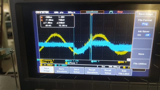
IMAGE1: grid Voltage, Output current spike.

Yellow - Grid voltage, Blue - output current.
(These waveforms are captured near micro pins).
IMAGE2: Yellow -Grid voltage, Blue - Output voltage.
CODE:
void pll_loop_run()
{
// Relay=!Relay;
Read_Inputs_Filtered(&v_ac_ref, &i_ac_fb);
//v_ac_re : it is voltage refernce bipolar signal -1 to 1
//i_ac_fb it is current feedback from the inveter lcl output using ct sensor
SPLL_1PH_SOGI_run(&spll1, v_ac_ref);
invSine=spll1.sine;
inv_stat_cnt++;
if(test_switch==0)
{
coeff_flag=1;
tune_flag=0;
}
//activatine the loop after some delay when switch is pressed
if(test_switch==0&&inv_stat_cnt>=100000)
{
// EPwm1Regs.DBCTL.bit.OUT_MODE = 3; //dead band enabled
// EPwm1Regs.AQCSFRC.bit.CSFA = 0; // Return to normal
// EPwm1Regs.AQCSFRC.bit.CSFB = 0;
//used for zero cross relay command is turned on at the -0.8 to -0.81 and enableing
// current loop at same instant
detect_zero_cross();
if ((invSinePrev <= (float32_t) (0.00))
&& (invSine > (float32_t) (0.00)))
{
zeroCrossDetectFlag = 1;
}
else
{
zeroCrossDetectFlag = 0;
}
if (clearInvTrip == 1 && zeroCrossDetectFlag == 1)
{
// EALLOW;
//clear oc fault
// EALLOW;
// EPwm1Regs.TZCLR.bit.DCAEVT1 = 1;
// EPwm1Regs.TZCLR.bit.OST = 1; //clear the event
// EPwm1Regs.TZCLR.bit.INT = 1;
// EDIS;
//end
// GpioDataRegs.GPACLEAR.bit.GPIO27=1;
// GpioDataRegs.GPACLEAR.bit.GPIO20 = 1;
// clearInvTrip = 0;
// closeILoopInv = 1;
}
// inv_stat_cnt=0;
}
invSinePrev = invSine;
// it is for switch disabled
if (test_switch == 1)
{
clearInvTrip = 1;
coeff_flag = 0;
curent_inc = 0.01;
oc_trip = 0;
GpioDataRegs.GPACLEAR.bit.GPIO20 = 1;
//clear oc fault
EALLOW;
EPwm1Regs.TZCLR.bit.DCAEVT1 = 1;
EPwm1Regs.TZCLR.bit.OST = 1; //clear the event
EPwm1Regs.TZCLR.bit.INT = 1;
EDIS;
//end
GpioDataRegs.GPACLEAR.bit.GPIO27 = 1;
EPwm1Regs.DBCTL.bit.OUT_MODE = 0; //dead band disabled temporarly
// forceing the pwm to low becuse by default we are getting negative voltage
// due to complementart signal
EPwm1Regs.AQSFRC.bit.RLDCSF = 0; // Load immediately
EPwm1Regs.AQCSFRC.bit.CSFA = 1; // Force EPWM1A low
EPwm1Regs.AQCSFRC.bit.CSFB = 1; // Force EPWM1B low
inv_stat_cnt = 0;
closeILoopInv = 0;
rlyConnect = 0;
}
if (closeILoopInv == 1)
{
//realase pwm
EPwm1Regs.DBCTL.bit.OUT_MODE = 3; //dead band enabled
EPwm1Regs.AQCSFRC.bit.CSFA = 0; // Return to normal
EPwm1Regs.AQCSFRC.bit.CSFB = 0;
current_ref_cnt++;
// this is for softstart of current refernce
if (current_ref_cnt > 10000)
{
current_ref_cnt = 0;
curent_inc += 0.01;
}
if (curent_inc > 0.1)
curent_inc = 0.1;
//curent_inc removed due to spikes
//invIoRefInst : generated currrent refernce using sine
invIoRefInst = 0.01 * spll1.sine;
voltage_error = invIoRefInst - i_ac_fb;
gi_out = DCL_runDF22_C1(&gi_pr1, voltage_error)
+ DCL_runDF22_C1(&gi_r3, voltage_error)
+ DCL_runDF22_C1(&gi_r5, voltage_error)
+ DCL_runDF22_C1(&gi_r7, voltage_error)
+ DCL_runDF22_C1(&gi_r9, voltage_error)
+ DCL_runDF22_C1(&pi, voltage_error);
gi_notch1_out = DCL_runDF22_C4(¬ch1, gi_out);
gi_notch2_out = DCL_runDF22_C4(¬ch2, gi_notch1_out);
gi_lead_lag_out = DCL_runDF22_C1(&gi_lead_lag, gi_notch2_out);
// INV_Current_PI_Loop(voltage_error);
invDutyPU = (gi_lead_lag_out + v_ac_ref)
/ (0.65f * ( VDCBUS_MAX_SENSE / VDC_NOMINAL)); //0.64 -> 400vdc. (400 / 620 = 0.64)
}
else
{
// duty=0
invDutyPU = 0;
// invDutyPU= (1.2*v_ac_ref)+v_ac_ref; //0.64 -> 400vdc. (400 / 620 = 0.64)
}
duty_percent = 50.0f + (invDutyPU*45.0f);
duty_percent = (duty_percent > 95.0f) ? 95.0f : duty_percent;
duty_percent = (duty_percent < 5.0f) ? 5.0f : duty_percent;
duty = (duty_percent / 100.0f) * TBPRD_VALUE;
EPwm1Regs.CMPA.half.CMPA = (Uint16) duty;
guiVbus = invVbusInst*VAC_MAX_SENSE;
guiVo = v_ac_ref*VDCBUS_MAX_SENSE;
guiIi = i_ac_fb*I_MAX_SENSE;
sine_mains.i =i_ac_fb;
sine_mains.v = v_ac_ref;
POWER_MEAS_SINE_ANALYZER_run(&sine_mains);
guiIrms = sine_mains.iRms*I_MAX_SENSE;
guiVrms = sine_mains.vRms*VAC_MAX_SENSE;
guiPrms = sine_mains.pRms*VAC_MAX_SENSE*I_MAX_SENSE;
guiPowerFactor = sine_mains.powerFactor;
guiVA = sine_mains.vaRms*VAC_MAX_SENSE*I_MAX_SENSE;
guiFreqAvg = sine_mains.acFreqAvg;
guiVema = sine_mains.vEma*VAC_MAX_SENSE;
acFreq_lpf = acFreq_lpf+(spll1.fo-acFreq_lpf)*0.00005;
}
void detect_zero_cross()
{
if ((invSinePrev <= (float) (0.00)) && (invSine > (float) (0.00)))
{
zeroCrossDetectFlag = 1;
}
else
{
zeroCrossDetectFlag = 0;
}
if (clearInvTrip==1 && zeroCrossDetectFlag==1)
{
EALLOW;
//clear oc fault
EALLOW;
EPwm1Regs.TZCLR.bit.DCAEVT1 = 1;
EPwm1Regs.TZCLR.bit.OST = 1; //clear the event
EPwm1Regs.TZCLR.bit.INT = 1;
EDIS;
//end
// GpioDataRegs.GPACLEAR.bit.GPIO27 = 1;
GpioDataRegs.GPACLEAR.bit.GPIO20=1;
clearInvTrip = 0;
// closeILoopInv = 1;
}
if(invSinePrev > -0.80 && invSine <-0.80)
{
if(rlyConnect == 0)
{
rlyConnect=1;
closeILoopInv = 1;
closeRelay();
}
}
// if (rlyConnect == 0)
// {
// openRelay();
// invVoRef = 0;
// invIiRef = 0;
// }
}
