Part Number: TMS320F28379D
Other Parts Discussed in Thread: C2000WARE
Tool/software:
Hello,
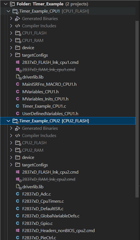
I am running the same code on CPU1 and CPU2 of the F28379D, and both are configured to execute from FLASH. The code mainly generates three sine waves and runs a 3-Phase SRF PLL routine.
-
On CPU1, the SRF PLL routine takes about 140 Clock cycles.
-
On CPU2, the same routine takes about 1300 Clock cycles.
Setup details:
-
A 10 kHz timer interrupt triggers the execution on both CPUs - Timer0 in CPU1 and Timer1 in CPU2.
-
Inside the ISR, the code performs the sine-wave generation and runs the 3-Phase SRF PLL.
-
The exact same code is used on both CPUs.
Issue:
CPU2 is approximately 10× slower than CPU1, even though both are running from FLASH with the same code and ISR setup.
Question:
What could cause CPU2 to execute much slower than CPU1 when both are running identical code from FLASH? Are there any specific memory configuration or wait-state considerations for CPU2 when executing from FLASH?
ISR routine in CPU1
__interrupt void timer0_isr(void)
{
    // Execute control algorithms
    // Toggle GPIO 22
    HWREG(GPIODATA_BASE + GPIO_O_GPATOGGLE) |= (uint32_t) 0x400000U;

    theta = theta + (TWO_PI * 50.0f * ISR_TIME_PERIOD);

    if (theta > TWO_PI) theta -= TWO_PI;

    Vgrid.Va = Vm * __cos(theta);
    Vgrid.Vb = Vm * __cos(theta-(TWO_PI / 3.0f));
    Vgrid.Vc = Vm * __cos(theta+(TWO_PI / 3.0f));

    Vgrid.Vab = Vgrid.Va - Vgrid.Vb;
    Vgrid.Vbc = Vgrid.Vb - Vgrid.Vc;

    SRF_PLL_MACRO(Vgrid);

    // Cleanup
    // Clear flag in timer module (optional - but better to do this)
    HWREGH(CPUTIMER0_BASE + CPUTIMER_O_TCR) |= 0x8000U;
    // Clear ACK bit in PIEACK register
    HWREGH(PIECTRL_BASE + PIE_O_ACK) |= (uint16_t) 0x1U;
}
ISR routine in CPU2
__interrupt void timer1_isr(void)
{
    // Execute control algorithms
    // Toggle GPIO 52
    GpioDataRegs.GPBTOGGLE.bit.GPIO52 = 1;

    theta = theta + (TWO_PI * 50.0f * ISR_TIME_PERIOD);

    if (theta > TWO_PI) theta -= TWO_PI;

    Vgrid.Va = Vm * __cos(theta);
    Vgrid.Vb = Vm * __cos(theta-(TWO_PI / 3.0f));
    Vgrid.Vc = Vm * __cos(theta+(TWO_PI / 3.0f));

    Vgrid.Vab = Vgrid.Va - Vgrid.Vb;
    Vgrid.Vbc = Vgrid.Vb - Vgrid.Vc;

    SRF_PLL_MACRO(Vgrid);


    // Cleanup
    // Clear flag in timer module
    CpuTimer1Regs.TCR.bit.TIF = 1;
}
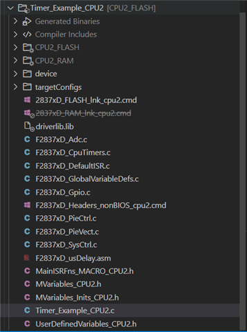
FLASH linker CMD files for both the CPU's are as below
2837xD_FLASH_lnk_cpu1.cmd file
MEMORY
{
PAGE 0 :  /* Program Memory */
          /* Memory (RAM/FLASH) blocks can be moved to PAGE1 for data allocation */
          /* BEGIN is used for the "boot to Flash" bootloader mode   */

   BEGIN           	: origin = 0x080000, length = 0x000002
   RAMM0           	: origin = 0x000123, length = 0x0002DD
   RAMD0           	: origin = 0x00B000, length = 0x000800
   RAMLS0          	: origin = 0x008000, length = 0x000800
   RAMLS1          	: origin = 0x008800, length = 0x000800
   RAMLS2      		: origin = 0x009000, length = 0x000800
   RAMLS3      		: origin = 0x009800, length = 0x000800
   RAMLS4      		: origin = 0x00A000, length = 0x000800
   RAMGS14          : origin = 0x01A000, length = 0x001000     /* Only Available on F28379D, F28377D, F28375D devices. Remove line on other devices. */
   RAMGS15          : origin = 0x01B000, length = 0x000FF8     /* Only Available on F28379D, F28377D, F28375D devices. Remove line on other devices. */

//   RAMGS15_RSVD     : origin = 0x01BFF8, length = 0x000008    /* Reserve and do not use for code as per the errata advisory "Memory: Prefetching Beyond Valid Memory" */

   RESET           	: origin = 0x3FFFC0, length = 0x000002

   /* Flash sectors */
   FLASHA           : origin = 0x080002, length = 0x001FFE	/* on-chip Flash */
   FLASHB           : origin = 0x082000, length = 0x002000	/* on-chip Flash */
   FLASHC           : origin = 0x084000, length = 0x002000	/* on-chip Flash */
   FLASHD           : origin = 0x086000, length = 0x002000	/* on-chip Flash */
   FLASHE           : origin = 0x088000, length = 0x008000	/* on-chip Flash */
   FLASHF           : origin = 0x090000, length = 0x008000	/* on-chip Flash */
   FLASHG           : origin = 0x098000, length = 0x008000	/* on-chip Flash */
   FLASHH           : origin = 0x0A0000, length = 0x008000	/* on-chip Flash */
   FLASHI           : origin = 0x0A8000, length = 0x008000	/* on-chip Flash */
   FLASHJ           : origin = 0x0B0000, length = 0x008000	/* on-chip Flash */
   FLASHK           : origin = 0x0B8000, length = 0x002000	/* on-chip Flash */
   FLASHL           : origin = 0x0BA000, length = 0x002000	/* on-chip Flash */
   FLASHM           : origin = 0x0BC000, length = 0x002000	/* on-chip Flash */
   FLASHN           : origin = 0x0BE000, length = 0x001FF0	/* on-chip Flash */

//   FLASHN_RSVD     : origin = 0x0BFFF0, length = 0x000010    /* Reserve and do not use for code as per the errata advisory "Memory: Prefetching Beyond Valid Memory" */

PAGE 1 : /* Data Memory */
         /* Memory (RAM/FLASH) blocks can be moved to PAGE0 for program allocation */

   BOOT_RSVD       : origin = 0x000002, length = 0x000121     /* Part of M0, BOOT rom will use this for stack */
   RAMM1           : origin = 0x000400, length = 0x0003F8     /* on-chip RAM block M1 */
//   RAMM1_RSVD      : origin = 0x0007F8, length = 0x000008     /* Reserve and do not use for code as per the errata advisory "Memory: Prefetching Beyond Valid Memory" */
   RAMD1           : origin = 0x00B800, length = 0x000800

   RAMLS5      : origin = 0x00A800, length = 0x000800

   RAMGS0      : origin = 0x00C000, length = 0x001000
   RAMGS1      : origin = 0x00D000, length = 0x001000
   RAMGS2      : origin = 0x00E000, length = 0x001000
   RAMGS3      : origin = 0x00F000, length = 0x001000
   RAMGS4      : origin = 0x010000, length = 0x001000
   RAMGS5      : origin = 0x011000, length = 0x001000
   RAMGS6      : origin = 0x012000, length = 0x001000
   RAMGS7      : origin = 0x013000, length = 0x001000
   RAMGS8      : origin = 0x014000, length = 0x001000
   RAMGS9      : origin = 0x015000, length = 0x001000
   RAMGS10     : origin = 0x016000, length = 0x001000

//   RAMGS11     : origin = 0x017000, length = 0x000FF8   /* Uncomment for F28374D, F28376D devices */

//   RAMGS11_RSVD : origin = 0x017FF8, length = 0x000008    /* Reserve and do not use for code as per the errata advisory "Memory: Prefetching Beyond Valid Memory" */

   RAMGS11     : origin = 0x017000, length = 0x001000     /* Only Available on F28379D, F28377D, F28375D devices. Remove line on other devices. */
   RAMGS12     : origin = 0x018000, length = 0x001000     /* Only Available on F28379D, F28377D, F28375D devices. Remove line on other devices. */
   RAMGS13     : origin = 0x019000, length = 0x001000     /* Only Available on F28379D, F28377D, F28375D devices. Remove line on other devices. */

   CPU2TOCPU1RAM   : origin = 0x03F800, length = 0x000400
   CPU1TOCPU2RAM   : origin = 0x03FC00, length = 0x000400
}

SECTIONS
{
   /* Allocate program areas: */
   .cinit              : > FLASHB      PAGE = 0, ALIGN(8)
   .text               : >> FLASHB | FLASHC | FLASHD | FLASHE      PAGE = 0, ALIGN(8)
   codestart           : > BEGIN       PAGE = 0, ALIGN(8)
   /* Allocate uninitalized data sections: */
   .stack              : > RAMM1       PAGE = 1
   .switch             : > FLASHB      PAGE = 0, ALIGN(8)
   .reset              : > RESET,      PAGE = 0, TYPE = DSECT /* not used, */

#if defined(__TI_EABI__)
   .init_array         : > FLASHB,       PAGE = 0,       ALIGN(8)
   .bss                : > RAMLS5,       PAGE = 1
   .bss:output         : > RAMLS3,       PAGE = 0
   .bss:cio            : > RAMLS5,       PAGE = 1
   .data               : > RAMLS5,       PAGE = 1
   .sysmem             : > RAMLS5,       PAGE = 1
   /* Initalized sections go in Flash */
   .const              : > FLASHF,       PAGE = 0,       ALIGN(8)
#else
   .pinit              : > FLASHB,       PAGE = 0,       ALIGN(8)
   .ebss               : >> RAMLS5 | RAMGS0 | RAMGS1,    PAGE = 1
   .esysmem            : > RAMLS5,       PAGE = 1
   .cio                : > RAMLS5,       PAGE = 1
   /* Initalized sections go in Flash */
   .econst             : >> FLASHF      PAGE = 0, ALIGN(8)
#endif

   Filter_RegsFile     : > RAMGS0,	   PAGE = 1

   SHARERAMGS0		: > RAMGS0,		PAGE = 1
   SHARERAMGS1		: > RAMGS1,		PAGE = 1
   SHARERAMGS2		: > RAMGS2,		PAGE = 1
   ramgs0           : > RAMGS0,     PAGE = 1
   ramgs1           : > RAMGS1,     PAGE = 1

#ifdef __TI_COMPILER_VERSION__
    #if __TI_COMPILER_VERSION__ >= 15009000
        #if defined(__TI_EABI__)
            .TI.ramfunc : {} LOAD = FLASHD,
                                 RUN = RAMLS0,
                                 LOAD_START(RamfuncsLoadStart),
                                 LOAD_SIZE(RamfuncsLoadSize),
                                 LOAD_END(RamfuncsLoadEnd),
                                 RUN_START(RamfuncsRunStart),
                                 RUN_SIZE(RamfuncsRunSize),
                                 RUN_END(RamfuncsRunEnd),
                                 PAGE = 0, ALIGN(8)
        #else
            .TI.ramfunc : {} LOAD = FLASHD,
                             RUN = RAMLS0,
                             LOAD_START(_RamfuncsLoadStart),
                             LOAD_SIZE(_RamfuncsLoadSize),
                             LOAD_END(_RamfuncsLoadEnd),
                             RUN_START(_RamfuncsRunStart),
                             RUN_SIZE(_RamfuncsRunSize),
                             RUN_END(_RamfuncsRunEnd),
                             PAGE = 0, ALIGN(8)
        #endif
    #else
   ramfuncs            : LOAD = FLASHD,
                         RUN = RAMLS0,
                         LOAD_START(_RamfuncsLoadStart),
                         LOAD_SIZE(_RamfuncsLoadSize),
                         LOAD_END(_RamfuncsLoadEnd),
                         RUN_START(_RamfuncsRunStart),
                         RUN_SIZE(_RamfuncsRunSize),
                         RUN_END(_RamfuncsRunEnd),
                         PAGE = 0, ALIGN(8)
    #endif

#endif

   /* The following section definitions are required when using the IPC API Drivers */
    GROUP : > CPU1TOCPU2RAM, PAGE = 1
    {
        PUTBUFFER
        PUTWRITEIDX
        GETREADIDX
    }

    GROUP : > CPU2TOCPU1RAM, PAGE = 1
    {
        GETBUFFER :    TYPE = DSECT
        GETWRITEIDX :  TYPE = DSECT
        PUTREADIDX :   TYPE = DSECT
    }

   /* The following section definition are for SDFM examples */
   Filter1_RegsFile : > RAMGS1,	PAGE = 1, fill=0x1111
   Filter2_RegsFile : > RAMGS2,	PAGE = 1, fill=0x2222
   Filter3_RegsFile : > RAMGS3,	PAGE = 1, fill=0x3333
   Filter4_RegsFile : > RAMGS4,	PAGE = 1, fill=0x4444
   Difference_RegsFile : >RAMGS5, 	PAGE = 1, fill=0x3333
}

/*
//===========================================================================
// End of file.
//===========================================================================
*/
2837xD_FLASH_lnk_cpu2.cmd file
MEMORY
{
PAGE 0 :
   /* BEGIN is used for the "boot to SARAM" bootloader mode   */

   BEGIN           	: origin = 0x080000, length = 0x000002
   RAMM0           	: origin = 0x0000A2, length = 0x00035E
   RAMD0           	: origin = 0x00B000, length = 0x000800
   RAMLS0          	: origin = 0x008000, length = 0x000800
   RAMLS1          	: origin = 0x008800, length = 0x000800
   RAMLS2      		: origin = 0x009000, length = 0x000800
   RAMLS3      		: origin = 0x009800, length = 0x000800
   RAMLS4      		: origin = 0x00A000, length = 0x000800
   RAMGS14          : origin = 0x01A000, length = 0x001000     /* Only Available on F28379D, F28377D, F28375D devices. Remove line on other devices. */
   RAMGS15          : origin = 0x01B000, length = 0x000FF8     /* Only Available on F28379D, F28377D, F28375D devices. Remove line on other devices. */

//   RAMGS15_RSVD     : origin = 0x01BFF8, length = 0x000008    /* Reserve and do not use for code as per the errata advisory "Memory: Prefetching Beyond Valid Memory" */

   RESET       		: origin = 0x3FFFC0, length = 0x000002

   /* Flash sectors */
   FLASHA           : origin = 0x080002, length = 0x001FFE	/* on-chip Flash */
   FLASHB           : origin = 0x082000, length = 0x002000	/* on-chip Flash */
   FLASHC           : origin = 0x084000, length = 0x002000	/* on-chip Flash */
   FLASHD           : origin = 0x086000, length = 0x002000	/* on-chip Flash */
   FLASHE           : origin = 0x088000, length = 0x008000	/* on-chip Flash */
   FLASHF           : origin = 0x090000, length = 0x008000	/* on-chip Flash */
   FLASHG           : origin = 0x098000, length = 0x008000	/* on-chip Flash */
   FLASHH           : origin = 0x0A0000, length = 0x008000	/* on-chip Flash */
   FLASHI           : origin = 0x0A8000, length = 0x008000	/* on-chip Flash */
   FLASHJ           : origin = 0x0B0000, length = 0x008000	/* on-chip Flash */
   FLASHK           : origin = 0x0B8000, length = 0x002000	/* on-chip Flash */
   FLASHL           : origin = 0x0BA000, length = 0x002000	/* on-chip Flash */
   FLASHM           : origin = 0x0BC000, length = 0x002000	/* on-chip Flash */
   FLASHN           : origin = 0x0BE000, length = 0x001FF0	/* on-chip Flash */

//   FLASHN_RSVD     : origin = 0x0BFFF0, length = 0x000010    /* Reserve and do not use for code as per the errata advisory "Memory: Prefetching Beyond Valid Memory" */

PAGE 1 :

   BOOT_RSVD       : origin = 0x000002, length = 0x0000A0     /* Part of M0, BOOT rom will use this for stack */
   RAMM1           : origin = 0x000400, length = 0x0003F8     /* on-chip RAM block M1 */
//   RAMM1_RSVD      : origin = 0x0007F8, length = 0x000008     /* Reserve and do not use for code as per the errata advisory "Memory: Prefetching Beyond Valid Memory" */
   RAMD1           : origin = 0x00B800, length = 0x000800

   RAMLS5          : origin = 0x00A800, length = 0x000800

   RAMGS0          : origin = 0x00C000, length = 0x001000
   RAMGS1          : origin = 0x00D000, length = 0x001000
   RAMGS2          : origin = 0x00E000, length = 0x001000
   CPU2TOCPU1RAM   : origin = 0x03F800, length = 0x000400
   CPU1TOCPU2RAM   : origin = 0x03FC00, length = 0x000400
}

SECTIONS
{
   /* Allocate program areas: */
   .cinit              : > FLASHB      PAGE = 0, ALIGN(8)
   //.text               : > FLASHB      PAGE = 0, ALIGN(8)
   .text               : >> FLASHB | FLASHC | FLASHD | FLASHE      PAGE = 0, ALIGN(8)
   codestart           : > BEGIN       PAGE = 0, ALIGN(8)

   /* Allocate uninitalized data sections: */
   .stack              : > RAMM1        PAGE = 1

   /* Initalized sections go in Flash */
   .switch             : > FLASHB      PAGE = 0, ALIGN(8)
   .reset           : > RESET,     PAGE = 0, TYPE = DSECT /* not used, */

#if defined(__TI_EABI__)
   .init_array         : > FLASHB,       PAGE = 0,       ALIGN(8)
   .bss                : > RAMLS5,       PAGE = 1
   .bss:output         : > RAMLS3,       PAGE = 0
   .bss:cio            : > RAMLS5,       PAGE = 1
   .data               : > RAMLS5,       PAGE = 1
   .sysmem             : > RAMLS5,       PAGE = 1
   /* Initalized sections go in Flash */
   .const              : > FLASHF,       PAGE = 0,       ALIGN(8)
#else
   .pinit              : > FLASHB,       PAGE = 0,       ALIGN(8)
   //.ebss               : >> RAMLS5 | RAMGS0 | RAMGS1,    PAGE = 1
   .ebss               : >> RAMLS5,    PAGE = 1
   .esysmem            : > RAMLS5,       PAGE = 1
   .cio                : > RAMLS5,       PAGE = 1
   /* Initalized sections go in Flash */
   .econst             : >> FLASHF       PAGE = 0, ALIGN(8)
#endif

   SHARERAMGS0		: > RAMGS0,		PAGE = 1
   SHARERAMGS1		: > RAMGS1,		PAGE = 1
   SHARERAMGS2		: > RAMGS2,		PAGE = 1

#ifdef __TI_COMPILER_VERSION__
    #if __TI_COMPILER_VERSION__ >= 15009000
        #if defined(__TI_EABI__)
            .TI.ramfunc : {} LOAD = FLASHD,
                                 RUN = RAMLS0,
                                 LOAD_START(RamfuncsLoadStart),
                                 LOAD_SIZE(RamfuncsLoadSize),
                                 LOAD_END(RamfuncsLoadEnd),
                                 RUN_START(RamfuncsRunStart),
                                 RUN_SIZE(RamfuncsRunSize),
                                 RUN_END(RamfuncsRunEnd),
                                 PAGE = 0, ALIGN(8)
        #else
            .TI.ramfunc : {} LOAD = FLASHD,
                             RUN = RAMLS0,
                             LOAD_START(_RamfuncsLoadStart),
                             LOAD_SIZE(_RamfuncsLoadSize),
                             LOAD_END(_RamfuncsLoadEnd),
                             RUN_START(_RamfuncsRunStart),
                             RUN_SIZE(_RamfuncsRunSize),
                             RUN_END(_RamfuncsRunEnd),
                             PAGE = 0, ALIGN(8)
        #endif
    #else
   ramfuncs            : LOAD = FLASHD,
                         RUN = RAMLS0,
                         LOAD_START(_RamfuncsLoadStart),
                         LOAD_SIZE(_RamfuncsLoadSize),
                         LOAD_END(_RamfuncsLoadEnd),
                         RUN_START(_RamfuncsRunStart),
                         RUN_SIZE(_RamfuncsRunSize),
                         RUN_END(_RamfuncsRunEnd),
                         PAGE = 0, ALIGN(8)
    #endif
#endif

   /* The following section definitions are required when using the IPC API Drivers */
    GROUP : > CPU2TOCPU1RAM, PAGE = 1
    {
        PUTBUFFER
        PUTWRITEIDX
        GETREADIDX
    }

    GROUP : > CPU1TOCPU2RAM, PAGE = 1
    {
        GETBUFFER :    TYPE = DSECT
        GETWRITEIDX :  TYPE = DSECT
        PUTREADIDX :   TYPE = DSECT
    }
}

/*
//===========================================================================
// End of file.
//===========================================================================
*/
I have also attached the full project file here for your reference.
Thank you
Vijaymahantesh V Surkod