Part Number: TMS320F28386D-Q1
Other Parts Discussed in Thread: SYSCONFIG
Hello,
My question relates to the hardware signals emanated by an FSI Rx core.
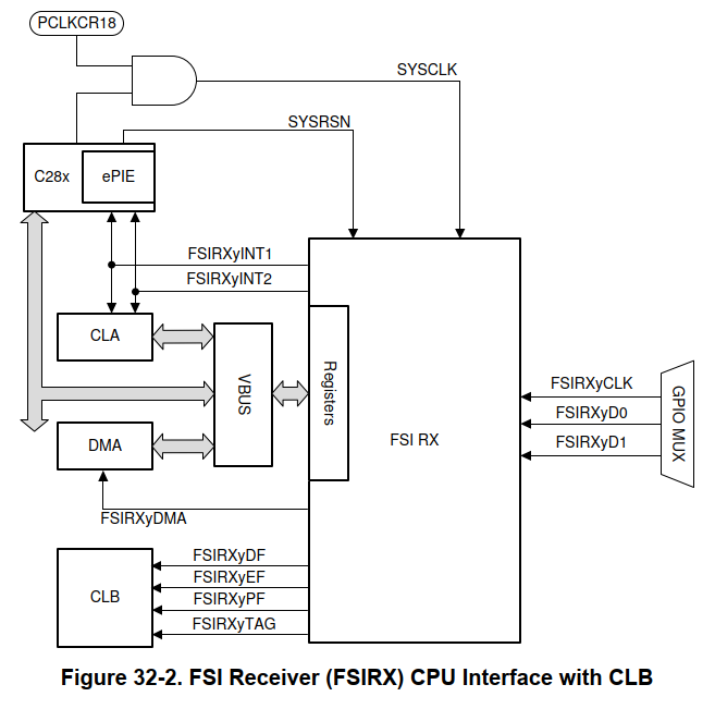
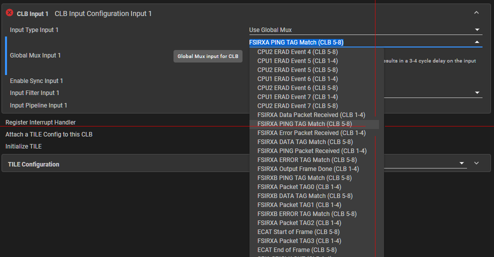
From the first excerpted figure 32-2 from the relevant TRM, we observe that four signals emanate from an FSI Rx core. From the second screenshot (CLB SysConfig tool) and also from Table 9-2 of the TRM, we observe that several additional FSI-related signals can be selected (e.g. "FSIRXA Ping Tag Match") as input sources to the CLBs.
While unfortunately none of this is spelled out in the TRM, one can deduce that the total list of FSI-Rx relevant signals available for use by a CLB input is likely a logical combination of the set of four "core" signals emanated by the FSI Rx core, as depicted in figure 32-2. For example, the "FSIRXA Ping Tag Match" is actually the logical intersection (AND) of the "FSIRxyPF" and "FSIRxyTAG" signals referred in Figure 32-2, assuming "FSIRxyTAG" in interpreted as logical signal representing tag match.
As a first order, confirmation (or otherwise correction) of this assumed behavior would be appreciated.
As a follow-on question, are these presumably logically-combined signals respective of each FSI Rx core that are made available as CLB inputs clocked in a common clock domain and time coordinated such that I can safely perform combinatorial logic in a CLB on a plurality of such signals from a given FSI Rx core?
As a concrete example, if I were to specify "FSIRXA Ping Tag Match" as a CLB input assigned to input 0 (let's denote i0), and "FSIRXA Ping Packet Received" as CLB input 1 (i1). Assuming each input has identical input synchronizer settings, could I safely (expectation of glitch-free operation) construct a LUT that performs i0 & !i1 to produce a signal that is effectively, "FSIRXA Ping Frame, No Tag Match"? Or will this potentially glitch, thereby requiring some higher-order logic?
What is the meaning of the "FSIRXA_PKT_TAG0/1/2/3" outlined in Table 9-2? There are no multiple tag match registers for the FSI Rx cores.
Thanks in advance,
David Michaud