This thread has been locked.

If you have a related question, please click the "Ask a related question" button in the top right corner. The newly created question will be automatically linked to this question.

TMS320F280039C: Unable to boot the device

Part Number: TMS320F280039C

Hello,

We are using F280039 MCU and intend to boot from flash. Pins GPIO24 and GPIO32 are pulled up to VDDIO through 22k Ohm resistor. During and after reset, GPIO24 is held at VDDIO but GPIO32 remains always LOW. Both GPIO24 and GPIO32 are connected to buffer pins which have high impedance during reset.

Unable to debug the trouble. Can you please help?

With regards,


Vijay Limaye

  • Hello,

    22k Ohms should be fine. Can you verify there are no shorts on the signal path to GPIO32? 

    Best,
    Matt

  • Hello,

    With power OFF, both, GPIO24 and GPIO32 show resistance of 23k Ohms to Ground (0V)..

    We inspected the GPIO32 trace under a magnifier, but no shorting with any other trace / component was observed.

    One other observation: the VDD supply shows only about 0.35V instead of 1.2V. VREGENZ pin of the MCU is connected to GND (verified).

    Are these two issue separate or related to each other?

    The MCU is also not able to connect with debug probe (XDS110).

    With regards,

    Vijay

  • We checked 3x boards and all 3 boards have these same issues.

    With regards,

    Vijay

  • Hello,

    One other observation: the VDD supply shows only about 0.35V instead of 1.2V. VREGENZ pin of the MCU is connected to GND (verified).

    Yes, this will have an affect on the core performance. With the internal VREG being used, you must place external bulk caps with values set forth in the DS: https://www.ti.com/document-viewer/TMS320F280039C/datasheet#GUID-9D2CEBE2-4430-4F99-87A2-C07098C07FA3/GUID-B83B02EC-3DA8-4AB8-9AA7-13DA2A4304AC

    Additionally, how much power are you providing to VDDIO? 

    Best,

    Matt

  • Hello,

    For VDD, we have 1x 22uF capacitor in addition to 4x 100nF capacitor.

    For VDDIO, we have 1x 22uF capacitor in addition to 4x 100nF capacitor..

    Please see below the snapshots from the schematic.

    With regards,

    Vijay

  • Hi Vijay,

    The decoupling and bulk capacitance looks fine to me for the power rails. The LD117 has a current capacity of 0.8A, are there any other components using the 3.3V rail? If so, please be sure to calculate the combined current consumption of all 3.3V devices and ensure it does not exceed the 0.8A

    Regards,

    Peter

  • Hi Peter,

    Thanks for the reply.

    Based on the datasheets of the ICs used on board, the total supply current drawn from 3.3V is about 180mA.Adding the current drawn by pull up resistors and other bias circuits, the total current drawn is less than 200mA for regulator with rating of 800mA.
    If we assume that some component has malfunctioned and is overloading the regulator, it will go into current limit and 3.3V output will drop. But 3.3V is steady. Also, as said earlier, these same issues have been observed on 3 boards that we checked. I think the question now is - if 3.3V (VDDIO) is steady, why is the MCU internal regulator for VDD not providing the required 1.2V?

    With regards,

    Vijay

  • Hello,

    We will continue to look into the internal regulator issue. Have you tried swapping out the device with a working one, and observe if the issue persists on the same board?

    Best,
    Matt

  • Hi Vijay,

    There is nothing sticking out to me from the information provided so that would result in an error like this. However, there does seem to be some issue possible with the VREG configuration. Is it possible to provide the remaining schematics (or specifically the full set of schematics related to Power, Clock, Reset, and Debug + circuits connected to GPIO24/32) to assist us further in debugging the issue?

    Best Regards,

    Zackary Fleenor

  • Hi,

    We can send the full schematic, however, from the information security point of view, we would like to send it to one specific official email id. Please let me know.

    With regards,

    Vijay

  • Hi Vijay,

    Understood. Please share with fleenor@ti.com, and we will continue digging into this issue.

    Best Regards,

    Zackary Fleenor

  • Hi Vijay,

    Thank you for providing the details. I have reviewed the schematic, and nothing is sticking out to me from a hardware perspective.

    I did note that GPIO24/32 are the default GPIO pins to configure the boot mode.

    What is the expectation in regards to the boot mode here? What is the configuration of BOOTPIN-CONFIG.BMPS[0:2]?

    What is the exact process followed for executing this test resulting in the failure to connect via XDS110?

    Best Regards,

    Zackary Fleenor

  • Hi,

    Please see the attached target configuration file used in the CCS project.

    Normally we click the "Debug" button in the CCS and the debug probe connects with the target board. If not, we open the target configuration file, check if the settings (debug probe type, device etc.) are correct and test the connection again after corrections as required. Beyond this, we have never faced any difficulty in connecting the debug probe to target board.

    I am not aware how to check the configuration of  BOOTPIN-CONFIG.BMPS[0:2]. Can you please let me know so that I can check and reply.

    With regards,

    Vijay Limaye

    TMS320F280039C.zip

  • Hi Vijay,

    Can you share the .syscfg file or related device configuration code for reference?

    What is the expected bootmode for the device?

    I will have a colleague provide a description for the best method to determine this configuration.

    Best Regards,

    Zackary Fleenor

  • Hello,

    I'm assuming you didn't program the DCSM OTP and are using the default flash boot option. There's no need to check the BOOTPIN-CONFIG registers Zackary mentioned.

    Did you ever check if the issue follows the device with a device swap?

    Best,
    Matt 

  • Hello,

    We didn't program the DCSM OTP and intend to use boot to flash option.

    We have checked this issue in 5 boards and found the same issue in all 5. We have not changed the device on any board. We will change the device on one board and test again.

    Please see attached the .syscfg file used in the CCS project. I think the code generated using this file will be executed if the device boots to flash. I doubt if the device boots to flash with VDD at 0.35V.

    With regards,

    Vijay Limaye

    cla_ex4_pwm_control.zip

  • Hello,

    Can you try probing XRSn to see if it ever releases high? I will continue to discuss this issue internally and get back to you by the end of the week.

    Best,

    Matt

  • Hello,

    During Power ON, XRSn goes high about 60ms after VDDIO has risen to 3.3V.

    Please see attached the waveform during power ON.

    Yellow trace is VDDIO and Red is XRSn - both 2V/div and 10ms/div.

    With regards,

    Vijay Limaye

  • Hello,

    We tested one board by replacing the MCU device with a new one, but no change in the results.

    With regards,

    Vijay Limaye

  • Hello,

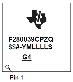
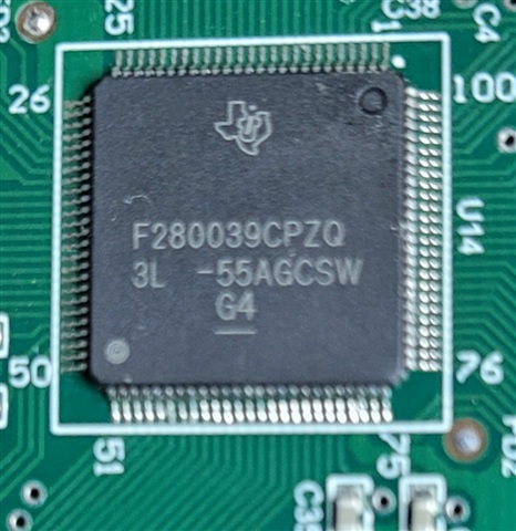
    We have a doubt about the orientation of the device mounted on board - the actual device has 2 markings which is creating confusion about pin 1 marking.

    Please see attached:

    • Snapshot from datasheet showing pin 1 marking (File F280039DatasheetSnapshot)
    • Actual device on board (File F280039Sample1)

    Request you to check and confirm if the device is correctly mounted on board.

    With regards,

    Vijay Limaye

  • Hello,

    I agree that is confusing. The pin 1 marking in the data sheet is correct, so the devices are oriented 180 degrees off from where pin 1 should be on your board.

    Best,

    Matt

  • Vijay,

    Just to re-state what Matt K has pointed out.  The grey/laser etched dot is pin one on this device, and appears in the correct orientation to the text on the device.  So you will need to rotate the device 180 degrees to line up the grey dot to the upper left orientation in your image.

    I am looking into when the dimple was added, we need to update the DS to show/clarify this marking, as I agree it is not helpful.

    Best,

    Matthew