This thread has been locked.

If you have a related question, please click the "Ask a related question" button in the top right corner. The newly created question will be automatically linked to this question.

TMS320F2800132: TMS320F2800132 Flash data cannot be written

Part Number: TMS320F2800132
Other Parts Discussed in Thread: TMS320F2800137, UNIFLASH

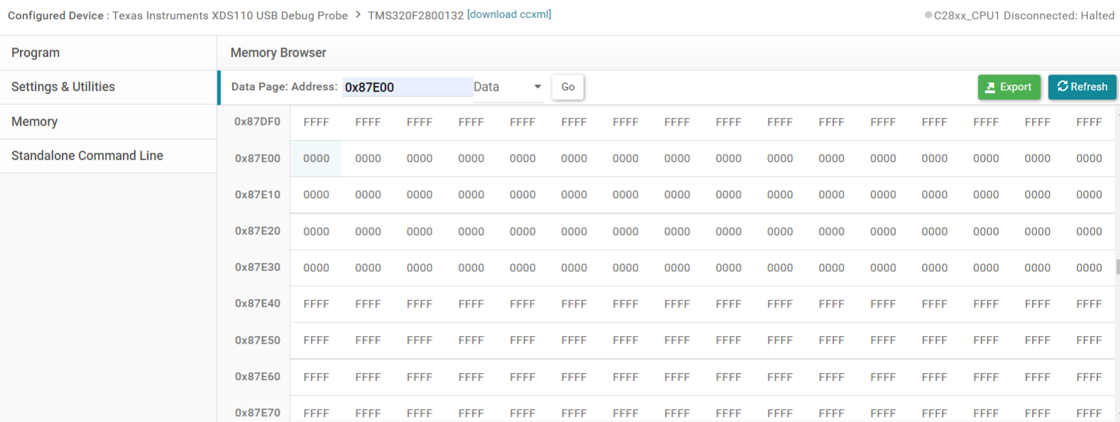
When applying the TMS320F2800132 chip, it was found that data could not be written in the Flash. However, when the SDK reference code was burned onto the TMS320F2800137 demo board, data could be written normally. But when the reference code was burned onto the TMS320F2800132 chip, data could not be written.
The erase and write functions are as follows. Attempts to increase the waiting time also failed to solve the problem. Please help me find out the cause of the problem. Thank you.

code.c 

Successfully(TMS320F2800137)

image.png


Failure(TMS320F2800132)

image.png

  • Hi Xin,

    The linker command file (.cmd) for a project that is intended to be used with F2800132 should be modified as the F2800132 device has less flash than the F2800137.

    Please see this post which explains the different ranges/cmd needed:  RE: TMS320F2800132: Sector Violation Issue  

    Best Regards,

    Marlyn

  • Hi Marlyn,

    thanks for your reply.I read the post you mentioned, and the problem described therein is different from the situation I encountered. I checked the 280013x_generic_flash_lnk.cmd file and found that the flash definition in it did not exceed the 64KB range. Additionally, the range I set did not exceed 0x88000. Here is a phenomenon for your reference. According to my understanding, if the flash cannot be written to, it should display 0xFFFF. However, after I wrote the data and then read the content at the corresponding address, the displayed value was 0x0000 instead of 0xFFFF. The individual verification of erasure is fine, but the writing has an anomaly. The content of 280013x_generic_flash_lnk.cmd is as follows.

    MEMORY
    {
    /*RAM0~RAM1:2KW = 4KB:0x00000000~0x00000800*/
    //RAMM0 : origin = 0x00000000, length = 0x00000400
    //RAMM1 : origin = 0x00000400, length = 0x00000400
    RAMM01 : origin = 0x00000000, length = 0x00000800
    /*RAMLS4~RAMLS7:8KW = 16KB:0x0000A000~0x0000BFFF*/
    //RAMLS4 : origin = 0x0000A000, length = 0x00000800
    //RAMLS5 : origin = 0x0000A800, length = 0x00000800
    //RAMLS6 : origin = 0x0000B000, length = 0x00000800
    //RAMLS7 : origin = 0x0000B800, length = 0x00000800
    RAMLS4567 : origin = 0x0000A000, length = 0x00002000
    /*RAMGS0:8KW = 16KB:0x0000C000~0x0000C7FF*/
    RAMGS0 : origin = 0x0000C000, length = 0x00000800
    /*BOOTROM:64KW:0x003F0000~x003F FFFF*/
    BOOTROM : origin = 0x003F0000, length = 0x00008000
    BOOTROM_EXT : origin = 0x003F8000, length = 0x00007FC0
    RESET : origin = 0x003FFFC0, length = 0x00000002
    /* Flash sectors */
    /* BANK 0 */
    // BEGIN : origin = 0x080000, length = 0x000002 /*code flash Begin */
    // FLASH_BANK0_SEC0 : origin = 0x080002, length = 0x000FFE /* on-chip Flash */
    // FLASH_BANK0_SEC1 : origin = 0x081000, length = 0x001000 /* on-chip Flash */
    // FLASH_BANK0_SEC2 : origin = 0x082000, length = 0x001000 /* on-chip Flash */
    // FLASH_BANK0_SEC3 : origin = 0x083000, length = 0x001000 /* on-chip Flash */
    // FLASH_BANK0_SEC4 : origin = 0x084000, length = 0x001000 /* on-chip Flash */
    // FLASH_BANK0_SEC5 : origin = 0x085000, length = 0x001000 /* on-chip Flash */
    // FLASH_BANK0_SEC6 : origin = 0x086000, length = 0x001000 /* on-chip Flash */
    // FLASH_BANK0_SEC7 : origin = 0x087000, length = 0x001000 /* on-chip Flash */
    #if 0
    BEGIN : origin = 0x080000, length = 0x000002 /*code flash Begin */
    FLASH_BANK2T6_SEC : origin = 0x080002, length = 0x006FEE /* App Flash */
    IAP_HEADER : origin = 0x086FF0, length = 0x000010 /* ISP Header*/
    FLASH_BANK7_SEC : origin = 0x087000, length = 0x001000 /* Eeprom Flash */
    #else
    BEGIN : origin = 0x082000, length = 0x000002 /*code flash Begin */
    FLASH_BANK2T6_SEC : origin = 0x082002, length = 0x002DEE /* App1 Flash */
    FLASH_BANK01_SEC : origin = 0x080002, length = 0x001FFE /* boot Flash */
    IAP_HEADER : origin = 0x084DF0, length = 0x000010 /* ISP Header*/
    FLASH_BANK5T7_SEC : origin = 0x085000, length = 0x002DF0 /* App2 Flash */
    IAP_HEADER1 : origin = 0x087DF0, length = 0x000010 /* ISP Header1*/
    BOOT_KEY : origin = 0x087E00, length = 0x000200 /* Eeprom Flash*/
    #endif
    DCSM_ZSEL_Z1_P0: origin = 0x078008, length = 0x000002
    DCSM_ZSEL_Z1_P1: origin = 0x07800C, length = 0x000002
    }


    SECTIONS
    {
    codestart : > BEGIN, ALIGN(8)
    .text : > FLASH_BANK2T6_SEC, ALIGN(8)
    .cinit : > FLASH_BANK2T6_SEC, ALIGN(8)
    .switch : > FLASH_BANK2T6_SEC, ALIGN(8)
    .reset : > RESET, TYPE = DSECT /* not used, */

    .stack : > RAMM01

    .init_array : > FLASH_BANK2T6_SEC, ALIGN(8)
    .bss : > RAMLS4567
    .bss:output : > RAMLS4567
    .bss:cio : > RAMLS4567
    .const : > FLASH_BANK2T6_SEC, ALIGN(8)
    .data : > RAMLS4567
    .sysmem : > RAMLS4567

    ramgs0 : > RAMGS0
    // IAP_BHeader : > IAP_HEADER , ALIGN(8)
    /* Allocate IQ math areas: */
    IQmath : > RAMLS4567
    IQmathTables : > RAMLS4567

    .TI.ramfunc : LOAD = FLASH_BANK2T6_SEC,
    RUN = RAMLS4567,
    LOAD_START(RamfuncsLoadStart),
    LOAD_SIZE(RamfuncsLoadSize),
    LOAD_END(RamfuncsLoadEnd),
    RUN_START(RamfuncsRunStart),
    RUN_SIZE(RamfuncsRunSize),
    RUN_END(RamfuncsRunEnd),
    ALIGN(8)
    dcsm_zsel_z1_1 : > DCSM_ZSEL_Z1_P0
    dcsm_zsel_z1_2 : > DCSM_ZSEL_Z1_P1
    }
    /*
    //===========================================================================
    // End of file.
    //===========================================================================
    */

    please suggest is there in problem with linker file , Pls help to solve the problem.

    Best Regards,

    Xin

  • Hi Marlyn,

    I have a 2800137 launchpad. Using the SDK reference code to program it onto the 2800137 board can be done successfully. However, when I changed the frequency of the SDK reference code to 100 MHz and programmed it onto my product (2800132), it failed to write successfully. Similarly, when I changed the frequency of my own engineering code to 120 MHz and programmed it onto the launchpad (2800137), it also failed to write properly. I have tried changing to different sectors, but the phenomenon remained the same.Could you please help me check if there is any problem with the configuration.Pls help to solve the problem.Thank you.

    Best Regards,

    Xin

  • Hi Xin,

    Are you able to replicate the issue with an example from the SDK? It is much easier to reproduce on my side if its a known base of SW that can be used. I don't see any issues with the ranges provided in your linker command file.

    However, when I changed the frequency of the SDK reference code to 100 MHz and programmed it onto my product (2800132), it failed to write successfully.

    Can you please describe how you are changing the frequency?

    Best Regards,

    Marlyn

  • Hi Marlyn,

    I re-modified the SDK reference code with a frequency of 100 MHz and burned it onto the 2800132 chip. It was able to write data normally. It seems that I made a mistake in my previous modification. The current problem is that when I changed my code to be the same as the reference code and burned it onto the 2800132 chip, the data it wrote was not what I expected it was all 0000. Here is the code after I removed the unnecessary parts from the reference code. When I burned this content onto the 2800132 chip, it was able to write data normally.

    #define DEVICE_SETCLOCK_CFG          (SYSCTL_OSCSRC_OSC2 | SYSCTL_IMULT(30) | \
                                          SYSCTL_REFDIV(1) | SYSCTL_ODIV(3) | \
                                          SYSCTL_SYSDIV(1) | SYSCTL_PLL_ENABLE | \
                                          SYSCTL_DCC_BASE_0)
    #define DEVICE_SYSCLK_FREQ          ((DEVICE_OSCSRC_FREQ * 30) / (1 * 3 * 1))
    #define FLASH_WRAPPER_PROGRAM_BASE         0x51000U 
    #define FLASH_O_CMDWEPROTA        0x11D0U   
    #define FLASH_O_CMDWEPROTB        0x11D4U  
    #define FlashTech_CPU0_BASE_ADDRESS ((Fapi_FmcRegistersType *)FLASH_WRAPPER_PROGRAM_BASE) 
    #define FLASH_WRAPPER_PROGRAM_BASE         0x51000U 
    
    
    void main(void)
    {
        memcpy(&RamfuncsRunStart, &RamfuncsLoadStart, (size_t)&RamfuncsLoadSize);
        SysCtl_setClock(DEVICE_SETCLOCK_CFG);
    
        Example_EraseSector(Bzero_Sector31_start);
        Example_ProgramUsingAutoECC(0x87E00, temp);
    }
    
    #pragma CODE_SECTION(Example_EraseSector, ".TI.ramfunc");
    void Example_EraseSector(uint32 u32Sectorx_Start)
    {
        Fapi_StatusType  oReturnCheck;
        Fapi_FlashStatusType  oFlashStatus;
        Fapi_FlashStatusWordType  oFlashStatusWord;
        // Initialize the Flash API by providing the Flash register base address
        // and operating frequency(in MHz).
        // This function is required to initialize the Flash API based on System
        // frequency before any other Flash API operation can be performed.
        // This function must also be called whenever System frequency or RWAIT is
        // changed.
        DINT;
        DRTM;
    //    DisableDog();
        oReturnCheck = Fapi_initializeAPI(FlashTech_CPU0_BASE_ADDRESS, DEVICE_SYSCLK_FREQ/1000000U);
        if(oReturnCheck != Fapi_Status_Success)
        {
            // Check Flash API documentation for possible errors
            Example_Error(oReturnCheck);
        }
        // Initialize the Flash banks and FMC for erase and program operations.
        // Fapi_setActiveFlashBank() function sets the Flash banks and FMC for
        // further Flash operations to be performed on the banks.
        oReturnCheck = Fapi_setActiveFlashBank(Fapi_FlashBank0);
        if(oReturnCheck != Fapi_Status_Success)
        {
            // Check Flash API documentation for possible errors
            Example_Error(oReturnCheck);
        }
        //
        // Erase the sector that is programmed in the above example
        // Erase Sector6
        //
    
        ClearFSMStatus();
        Fapi_setupBankSectorEnable(FLASH_WRAPPER_PROGRAM_BASE+FLASH_O_CMDWEPROTA, 0x13FFFF00);
        Fapi_setupBankSectorEnable(FLASH_WRAPPER_PROGRAM_BASE+FLASH_O_CMDWEPROTB, 0x00000080);
    
        oReturnCheck = Fapi_issueAsyncCommandWithAddress(Fapi_EraseSector,
                       (uint32 *)u32Sectorx_Start);
    
        //
        // Wait until FSM is done with erase sector operation
        //
        while (Fapi_checkFsmForReady() != Fapi_Status_FsmReady){}
    
        if(oReturnCheck != Fapi_Status_Success)
        {
            //
            // Check Flash API documentation for possible errors
            //
            Example_Error(oReturnCheck);
        }
    
        //
        // Read FMSTAT register contents to know the status of FSM after
        // erase command to see if there are any erase operation related errors
        //
        oFlashStatus = Fapi_getFsmStatus();
        if(oFlashStatus != 3)
        {
            //
            // Check Flash API documentation for FMSTAT and debug accordingly
            // Fapi_getFsmStatus() function gives the FMSTAT register contents.
            // Check to see if any of the EV bit, ESUSP bit, CSTAT bit or
            // VOLTSTAT bit is set (Refer to API documentation for more details).
            //
            FMSTAT_Fail();
        }
    
        //
        // Verify that Sector6 is erased
        //
        oReturnCheck = Fapi_doBlankCheck((uint32 *)u32Sectorx_Start,
                       0x800U,
                       &oFlashStatusWord);
    
        if(oReturnCheck != Fapi_Status_Success)
        {
            // Check Flash API documentation for error info
            Example_Error(oReturnCheck);
        }
    //    ClrDog();
    //    EnableDog();
        EINT;
        ERTM;
    }
    
    #pragma CODE_SECTION(Example_ProgramUsingAutoECC, ".TI.ramfunc");
    void Example_ProgramUsingAutoECC(uint32 u32ReadWriteAddr, uint16 *pu16Buf)
    {
        uint32 u32Index = 0;
        uint16 i = 0;
        Fapi_StatusType             oReturnCheck;
        Fapi_FlashStatusType        oFlashStatus;
        Fapi_FlashStatusWordType    oFlashStatusWord;
        // Initialize the Flash API by providing the Flash register base address
        // and operating frequency(in MHz).
        // This function is required to initialize the Flash API based on System
        // frequency before any other Flash API operation can be performed.
        // This function must also be called whenever System frequency or RWAIT is
        // changed.
        DINT;
        DRTM;
    //    DisableDog();
    
        oReturnCheck = Fapi_initializeAPI(FlashTech_CPU0_BASE_ADDRESS, DEVICE_SYSCLK_FREQ/1000000U);
        if(oReturnCheck != Fapi_Status_Success)
        {
            // Check Flash API documentation for possible errors
            Example_Error(oReturnCheck);
        }
        // Initialize the Flash banks and FMC for erase and program operations.
        // Fapi_setActiveFlashBank() function sets the Flash banks and FMC for
        // further Flash operations to be performed on the banks.
        oReturnCheck = Fapi_setActiveFlashBank(Fapi_FlashBank0);
        if(oReturnCheck != Fapi_Status_Success)
        {
            // Check Flash API documentation for possible errors
            Example_Error(oReturnCheck);
        }
        //
        // A data buffer of max 8 16-bit words can be supplied to the program
        // function.
        // Each word is programmed until the whole buffer is programmed or a
        // problem is found. However to program a buffer that has more than 8
        // words, program function can be called in a loop to program 8 words for
        // each loop iteration until the whole buffer is programmed.
        //
        // Remember that the main array flash programming must be aligned to
        // 64-bit address boundaries and each 64 bit word may only be programmed
        // once per write/erase cycle.  Meaning the length of the data buffer
        // (3rd parameter for Fapi_issueProgrammingCommand() function) passed
        // to the program function can only be either 4 or 8.
        //
        // Program data in Flash using "AutoEccGeneration" option.
        // When AutoEccGeneration option is used, Flash API calculates ECC for the
        // given 64-bit data and programs it along with the 64-bit main array data.
        // Note that any unprovided data with in a 64-bit data slice
        // will be assumed as 1s for calculating ECC and will be programmed.
        //
        // Note that data buffer (Buffer) is aligned on 64-bit boundary for verify
        // reasons.
        //
        // Monitor ECC address for Sector6 while programming with AutoEcc mode.
        //
        // In this example, 0x100 bytes are programmed in Flash Sector6
        // along with auto-generated ECC.
        //
        for(i = 0;i < WORDS_IN_FLASH_BUFFER1;i++)
        {
            Buffer[i] =  0x1111;//pu16Buf[i];
        }
        for(i=0, u32Index = u32ReadWriteAddr;
           (u32Index < (u32ReadWriteAddr + WORDS_IN_FLASH_BUFFER1));
           i+= 8, u32Index+= 8)
        {
            ClearFSMStatus();
            Fapi_setupBankSectorEnable(FLASH_WRAPPER_PROGRAM_BASE+FLASH_O_CMDWEPROTA, 0x13FFFF00);
            Fapi_setupBankSectorEnable(FLASH_WRAPPER_PROGRAM_BASE+FLASH_O_CMDWEPROTB, 0x00000080);
    
            oReturnCheck = Fapi_issueProgrammingCommand((uint32 *)u32Index,Buffer+i,
                                                   8, 0, 0, Fapi_AutoEccGeneration);
            //
            // Wait until the Flash program operation is over
            //
            while(Fapi_checkFsmForReady() == Fapi_Status_FsmBusy);
            if(oReturnCheck != Fapi_Status_Success)
            {
                //
                // Check Flash API documentation for possible errors
                //
                Example_Error(oReturnCheck);
            }
            //
            // Read FMSTAT register contents to know the status of FSM after
            // program command to see if there are any program operation related
            // errors
            //
            oFlashStatus = Fapi_getFsmStatus();
            if(oFlashStatus != 3)
            {
                //
                //Check FMSTAT and debug accordingly
                //
                FMSTAT_Fail();
            }
    
            //
            // Verify the programmed values.  Check for any ECC errors.
            //
            oReturnCheck = Fapi_doVerify((uint32 *)u32Index,
                                         4, (uint32 *)(uint32)(Buffer + i),
                                         &oFlashStatusWord);
    
    //        oReturnCheck = Fapi_doVerify((uint32 *)u32Index,
    //                                     4, Buffer32+(i/2),
    //                                     &oFlashStatusWord);
            if(oReturnCheck != Fapi_Status_Success)
            {
                //
                // Check Flash API documentation for possible errors
                //
                Example_Error(oReturnCheck);
            }
        }
    //    ClrDog();
    //    EnableDog();
        EINT;
        ERTM;
    }

    This is my code. I modified it to be the same as the SDK reference code, but I couldn't write the expected value.

    #define DEVICE_SETCLOCK_CFG          (SYSCTL_OSCSRC_OSC2 | SYSCTL_IMULT(30) | \
                                          SYSCTL_REFDIV(1) | SYSCTL_ODIV(3) | \
                                          SYSCTL_SYSDIV(1) | SYSCTL_PLL_ENABLE | \
                                          SYSCTL_DCC_BASE_0)
    #define DEVICE_SYSCLK_FREQ          ((DEVICE_OSCSRC_FREQ * 30) / (1 * 3 * 1))
    #define FLASH_WRAPPER_PROGRAM_BASE         0x51000U 
    #define FLASH_O_CMDWEPROTA        0x11D0U   
    #define FLASH_O_CMDWEPROTB        0x11D4U  
    #define FlashTech_CPU0_BASE_ADDRESS ((Fapi_FmcRegistersType *)FLASH_WRAPPER_PROGRAM_BASE) 
    #define FLASH_WRAPPER_PROGRAM_BASE         0x51000U 
    
    
    int main(void)
    {
        memcpy(&RamfuncsRunStart, &RamfuncsLoadStart, (size_t)&RamfuncsLoadSize);
        SysCtl_setClock(DEVICE_SETCLOCK_CFG);
    
        Example_EraseSector(Bzero_Sector31_start);
        Example_ProgramUsingAutoECC(0x87E00, temp);
    
    //    /*Init Peripherals*/
    //    InitAllApp();
    //    while(1)
    //    {
    //        ClrDog();
    //        RouHandlerCtlLibrary ();
    //        ISPWaitApp();
    //        DecodeSecInformationApp ();
    //        CheckHeaderApp();
    //        IrefoffsetEnableFlagApp();
    //        IrefoffsetEnableCheckApp();
    //    }
    }
    
    #pragma CODE_SECTION(Example_EraseSector, ".TI.ramfunc");
    void Example_EraseSector(uint32 u32Sectorx_Start)
    {
        Fapi_StatusType  oReturnCheck;
        Fapi_FlashStatusType  oFlashStatus;
        Fapi_FlashStatusWordType  oFlashStatusWord;
        // Initialize the Flash API by providing the Flash register base address
        // and operating frequency(in MHz).
        // This function is required to initialize the Flash API based on System
        // frequency before any other Flash API operation can be performed.
        // This function must also be called whenever System frequency or RWAIT is
        // changed.
        DINT;
        DRTM;
    //    DisableDog();
        oReturnCheck = Fapi_initializeAPI(FlashTech_CPU0_BASE_ADDRESS, DEVICE_SYSCLK_FREQ/1000000U);
        if(oReturnCheck != Fapi_Status_Success)
        {
            // Check Flash API documentation for possible errors
            Example_Error(oReturnCheck);
        }
        // Initialize the Flash banks and FMC for erase and program operations.
        // Fapi_setActiveFlashBank() function sets the Flash banks and FMC for
        // further Flash operations to be performed on the banks.
        oReturnCheck = Fapi_setActiveFlashBank(Fapi_FlashBank0);
        if(oReturnCheck != Fapi_Status_Success)
        {
            // Check Flash API documentation for possible errors
            Example_Error(oReturnCheck);
        }
        //
        // Erase the sector that is programmed in the above example
        // Erase Sector6
        //
    
        ClearFSMStatus();
        Fapi_setupBankSectorEnable(FLASH_WRAPPER_PROGRAM_BASE+FLASH_O_CMDWEPROTA, 0x13FFFF00);
        Fapi_setupBankSectorEnable(FLASH_WRAPPER_PROGRAM_BASE+FLASH_O_CMDWEPROTB, 0x00000080);
    
        oReturnCheck = Fapi_issueAsyncCommandWithAddress(Fapi_EraseSector,
                       (uint32 *)u32Sectorx_Start);
    
        //
        // Wait until FSM is done with erase sector operation
        //
        while (Fapi_checkFsmForReady() != Fapi_Status_FsmReady){}
    
        if(oReturnCheck != Fapi_Status_Success)
        {
            //
            // Check Flash API documentation for possible errors
            //
            Example_Error(oReturnCheck);
        }
    
        //
        // Read FMSTAT register contents to know the status of FSM after
        // erase command to see if there are any erase operation related errors
        //
        oFlashStatus = Fapi_getFsmStatus();
        if(oFlashStatus != 3)
        {
            //
            // Check Flash API documentation for FMSTAT and debug accordingly
            // Fapi_getFsmStatus() function gives the FMSTAT register contents.
            // Check to see if any of the EV bit, ESUSP bit, CSTAT bit or
            // VOLTSTAT bit is set (Refer to API documentation for more details).
            //
            FMSTAT_Fail();
        }
    
        //
        // Verify that Sector6 is erased
        //
        oReturnCheck = Fapi_doBlankCheck((uint32 *)u32Sectorx_Start,
                       0x800U,
                       &oFlashStatusWord);
    
        if(oReturnCheck != Fapi_Status_Success)
        {
            // Check Flash API documentation for error info
            Example_Error(oReturnCheck);
        }
    //    ClrDog();
    //    EnableDog();
        EINT;
        ERTM;
    }
    
    #pragma CODE_SECTION(Example_ProgramUsingAutoECC, ".TI.ramfunc");
    void Example_ProgramUsingAutoECC(uint32 u32ReadWriteAddr, uint16 *pu16Buf)
    {
        uint32 u32Index = 0;
        uint16 i = 0;
        Fapi_StatusType             oReturnCheck;
        Fapi_FlashStatusType        oFlashStatus;
        Fapi_FlashStatusWordType    oFlashStatusWord;
        // Initialize the Flash API by providing the Flash register base address
        // and operating frequency(in MHz).
        // This function is required to initialize the Flash API based on System
        // frequency before any other Flash API operation can be performed.
        // This function must also be called whenever System frequency or RWAIT is
        // changed.
        DINT;
        DRTM;
    //    DisableDog();
    
        oReturnCheck = Fapi_initializeAPI(FlashTech_CPU0_BASE_ADDRESS, DEVICE_SYSCLK_FREQ/1000000U);
        if(oReturnCheck != Fapi_Status_Success)
        {
            // Check Flash API documentation for possible errors
            Example_Error(oReturnCheck);
        }
        // Initialize the Flash banks and FMC for erase and program operations.
        // Fapi_setActiveFlashBank() function sets the Flash banks and FMC for
        // further Flash operations to be performed on the banks.
        oReturnCheck = Fapi_setActiveFlashBank(Fapi_FlashBank0);
        if(oReturnCheck != Fapi_Status_Success)
        {
            // Check Flash API documentation for possible errors
            Example_Error(oReturnCheck);
        }
        //
        // A data buffer of max 8 16-bit words can be supplied to the program
        // function.
        // Each word is programmed until the whole buffer is programmed or a
        // problem is found. However to program a buffer that has more than 8
        // words, program function can be called in a loop to program 8 words for
        // each loop iteration until the whole buffer is programmed.
        //
        // Remember that the main array flash programming must be aligned to
        // 64-bit address boundaries and each 64 bit word may only be programmed
        // once per write/erase cycle.  Meaning the length of the data buffer
        // (3rd parameter for Fapi_issueProgrammingCommand() function) passed
        // to the program function can only be either 4 or 8.
        //
        // Program data in Flash using "AutoEccGeneration" option.
        // When AutoEccGeneration option is used, Flash API calculates ECC for the
        // given 64-bit data and programs it along with the 64-bit main array data.
        // Note that any unprovided data with in a 64-bit data slice
        // will be assumed as 1s for calculating ECC and will be programmed.
        //
        // Note that data buffer (Buffer) is aligned on 64-bit boundary for verify
        // reasons.
        //
        // Monitor ECC address for Sector6 while programming with AutoEcc mode.
        //
        // In this example, 0x100 bytes are programmed in Flash Sector6
        // along with auto-generated ECC.
        //
        for(i = 0;i < WORDS_IN_FLASH_BUFFER1;i++)
        {
            Buffer[i] =  0x1111;//pu16Buf[i];
        }
        for(i=0, u32Index = u32ReadWriteAddr;
           (u32Index < (u32ReadWriteAddr + WORDS_IN_FLASH_BUFFER1));
           i+= 8, u32Index+= 8)
        {
            ClearFSMStatus();
            Fapi_setupBankSectorEnable(FLASH_WRAPPER_PROGRAM_BASE+FLASH_O_CMDWEPROTA, 0x13FFFF00);
            Fapi_setupBankSectorEnable(FLASH_WRAPPER_PROGRAM_BASE+FLASH_O_CMDWEPROTB, 0x00000080);
    
            oReturnCheck = Fapi_issueProgrammingCommand((uint32 *)u32Index,Buffer+i,
                                                   8, 0, 0, Fapi_AutoEccGeneration);
            //
            // Wait until the Flash program operation is over
            //
            while(Fapi_checkFsmForReady() == Fapi_Status_FsmBusy);
            if(oReturnCheck != Fapi_Status_Success)
            {
                //
                // Check Flash API documentation for possible errors
                //
                Example_Error(oReturnCheck);
            }
            //
            // Read FMSTAT register contents to know the status of FSM after
            // program command to see if there are any program operation related
            // errors
            //
            oFlashStatus = Fapi_getFsmStatus();
            if(oFlashStatus != 3)
            {
                //
                //Check FMSTAT and debug accordingly
                //
                FMSTAT_Fail();
            }
    
            //
            // Verify the programmed values.  Check for any ECC errors.
            //
            oReturnCheck = Fapi_doVerify((uint32 *)u32Index,
                                         4, (uint32 *)(uint32)(Buffer + i),
                                         &oFlashStatusWord);
    
    //        oReturnCheck = Fapi_doVerify((uint32 *)u32Index,
    //                                     4, Buffer32+(i/2),
    //                                     &oFlashStatusWord);
            if(oReturnCheck != Fapi_Status_Success)
            {
                //
                // Check Flash API documentation for possible errors
                //
                Example_Error(oReturnCheck);
            }
        }
    //    ClrDog();
    //    EnableDog();
        EINT;
        ERTM;
    }

    Is this a problem with my configuration? Please help me point it out. Thank you!

    Best Regards,

    Xin

  • Hi Xin,

    Just to confirm, you are using the same physical F2800132 device to load both the demo code and your code? I did a diff between the two files you shared and the only difference was that in the demo code main function is void main() where as in your code its int main(). This should not cause the issue that you are seeing. Are you doing any other operation in between loading both of these programs such as a power cycle? Also, if you view the memory content in CCS, does it match with what you are seeing with UniFlash?

    Best Regards,

    Marlyn

  • Hi Marlyn,

    Thank you for your reply.I have identified the cause of the Flash write exception. In the reference code, the address of the array "buffer" is defined as 0x0000A000, and its length is 0x00001FF8, as shown below.


    In my code, the address of the array "buffer" is defined as 0x0000C000, and its length is 0x00000800. as shown below.


    After modifying the "buffer" address, the flash can write data normally. I have verified that the length of the data is not out of range. Are there any differences between these two addresses? Why is the data within the range of 0x0000C000 considered abnormal? Thank you.

    Best Regards,

    Xin

  • Hi Xin,

    In my code, the address of the array "buffer" is defined as 0x0000C000, and its length is 0x00000800. as shown below.

    I am glad that you were able to identify the issue and get your code programmed correctly. May I ask why you were creating a new RAMGS0 section with the specified addressed? RAMLS1 address of 0x0000A000 is the correct location for the LS1 RAM. 

    Best Regards,

    Marlyn