


Part Number: TMS320F28P550SJ
Hi experts,
I found some descripiton mismatch in f28p55 TRM
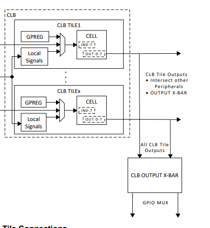
In the picture, the CLB out connect to OUTPUT-XBAR and CLB OUTPUT X-BAR
However, in X-BAR chatper, there is no CLB OUTPUT X-BAR table. It seems that the OUTPUT-XBAR table is the same with CLB OUTPUT X-BAR, because here are two OUTPUT_XBAR_REGS
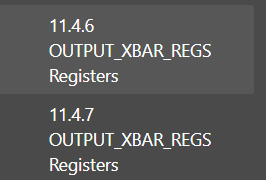
I double check the Table 11-5. Output X-BAR Mux Configuration Table and Table 30-4. CLB Output Signal Multiplexer Table
In table 30-4
CLB1_OUT12-All XBAR-G1.2
CLB1_OUT13-All XBAR-G3.2
CLB2_OUT12-All XBAR-G5.2
CLB2_OUT13-All XBAR-G7.2
In table 11-5, G1.2, 3.2, 5.2 and 7.2 are all reserved.
Q1: Does it means some MUX choices in Table 11-5 are reserved for CLB output? In Table 30-4, there four CLB Output Signal connecting to All XBAR. Does it means each tile can output 2 signals to GPIO pin?
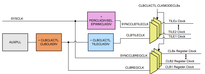
There is no EPWMCLDIV in PRECLKDIVSEL register.
Q2: SYNCCLBTILECLK can only be set as the same frequercny with SYSCLK?
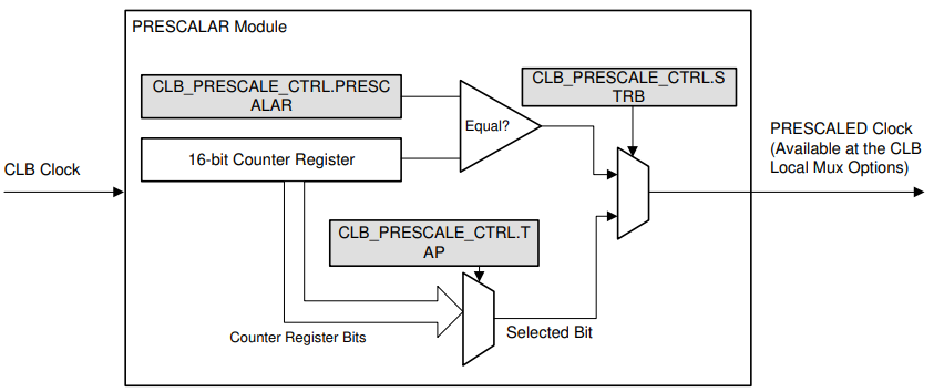
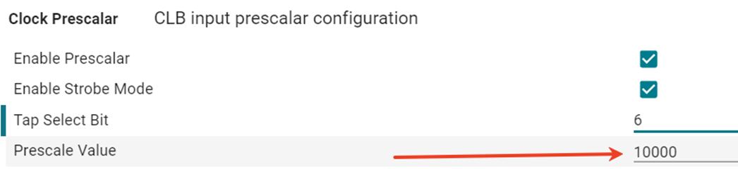
Q3: Our customer FENGTIAN feedback that they need set the large value to prescale value, the CLB clock can out put Square wave signal, is it normal?
In INTPULSEPOS bit, it describes that Interrupt pulse generation occurs at the end of the conversion, 1 cycle prior to the ADC result latching into its result register.

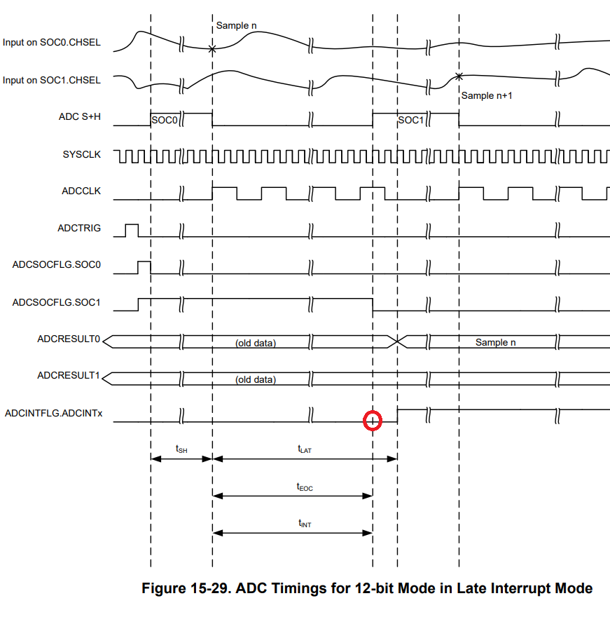
Q4: Should The interrupt signal be triggerred on the red circle?
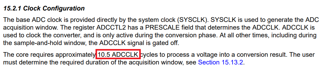
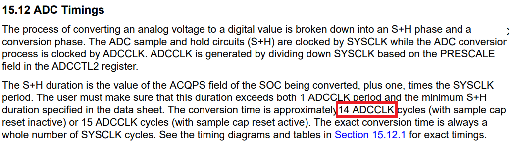
Q5: Which conversion time estimation is correct?
Thanks,
Leo
