


Part Number: TMS320F28P650DK
Other Parts Discussed in Thread: OPA328, REF34-Q1, OPA388-Q1
Hi,
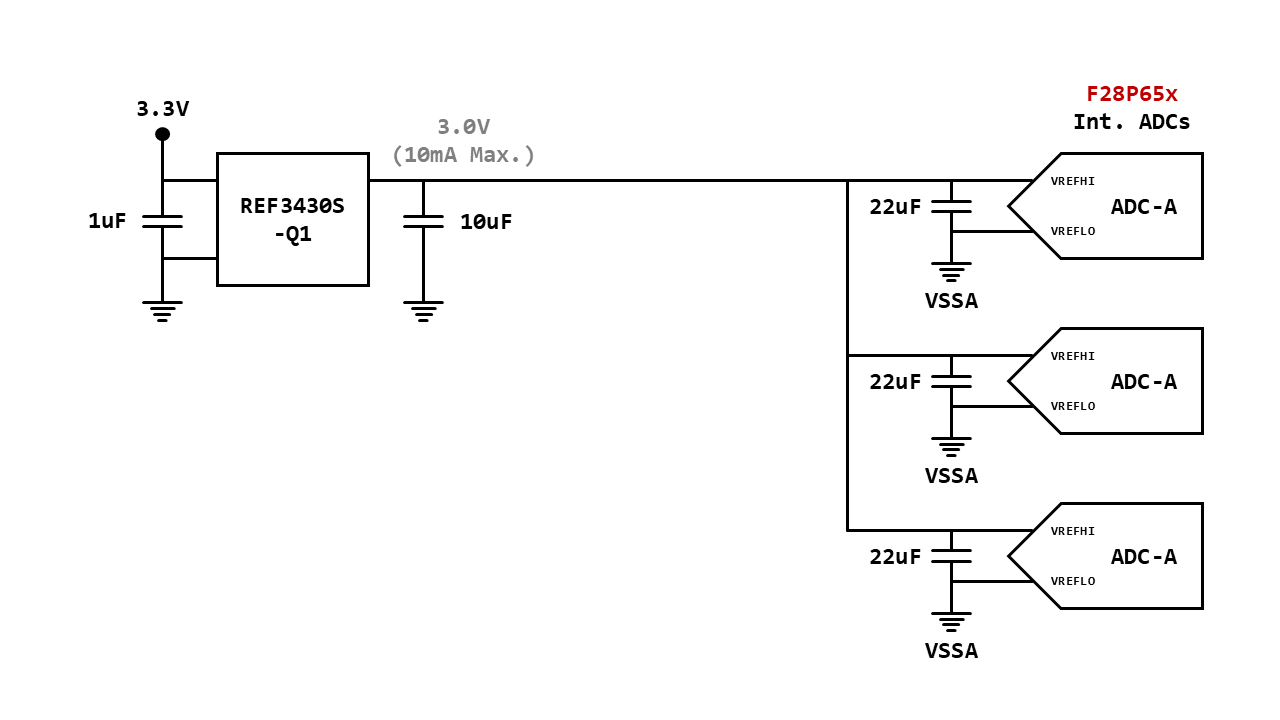
I plan to configure the external reference voltage circuit as follows to drive the on-chip ADC module of the F28P650DK9 MCU in 12-bit or 16-bit mode.
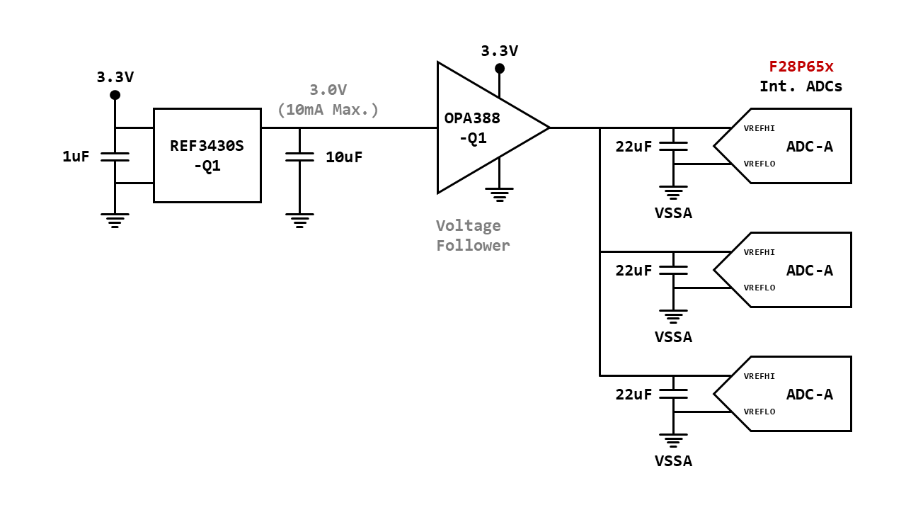
While proceeding with the relevant design, I searched for reference materials and found the 'VREFHI Driver Design for C2000 ADCs (spraby5)' application note. I reviewed its contents. That document explains that when designing the VREFHI driver circuit, using an Op. Amp.(OPA328) with zero-crossover technology as a voltage follower for the reference voltage output can drive the C2000 MCU on-chip ADCs with best performance.
In my opinion, there shouldn't be a major issue if I connect the voltage output of the REF34-Q1 component directly to the F28P65x's VREFHI port via a bypass capacitor, provided the distance between the reference voltage source and the F28P65x's VREFHI input port is minimized.
I would like to know if there is documentation that explains the difference between the two circuits(Unbuffered Reference vs. Buffered Reference) mentioned in the spraby5 application note in detail, focusing on the ADC result quality. Alternatively, I'm curious if there is any documentation that explains the potential problems or error rates that could occur when using the unbuffered reference circuit to operate the F28P65x's on-chip ADC modules in 16-bit differential input mode.
Finally, if the use of a voltage follower for the reference voltage output is strongly recommended, please check whether the OPA388-Q1 can be used instead of the OPA328 recommended in the application note.
Best regards,
Sang-il

