This thread has been locked.

If you have a related question, please click the "Ask a related question" button in the top right corner. The newly created question will be automatically linked to this question.

TMS320F28375D: Why Was Only the Lower 16 Bytes Referenced After Defining Argument 1 as 32 Bytes in a Function?

Genius 3215 points

Part Number: TMS320F28375D
Other Parts Discussed in Thread: C2000WARE

Hi All,

In the function, argument 1 was defined as 32 bytes, but after the function call, only the lower 16 bytes of argument 1 were referenced.
After changing the order of arguments 1 and 2, the reference register became one that supports 32 bytes, and the correct value could be accessed.

image.png

image.png

Why did the initial argument setting result in a register that could only reference the lower 16 bytes?

Best Regards,

Ito

  • For the source file that contains the function FlashErase, please follow the directions in the article How to Submit a Compiler Test Case.

    Thanks and regards,

    -George

  • Hi George,

    Thank you for your reply.

    I apologize for the delayed response.
    I will share the compiler information (build version and build log) via a private message.
    If there is anything missing in the content, please kindly let me know.

    Best Regards,
    Ito
  • Hi George,

    I sent a .pp file via private message.

    Best Regards,

    Ito

  • Thank you for the test case.  I don't see any problems in the assembly instructions generated by the compiler.  When you run the code, does it act the way you expect?  

    I do see a problem in the Dwarf debug information the compiler generates for CCS, and that problem shows up in the CCS display of the variable address, while having no effect on the execution of the overall system.  Do you agree?

    Thanks and regards,

    -George

  • Hi George,

    Thank you for your reply.

    The arguments have been successfully verified without any issues.
    However, the current phenomenon occurs when calling the Flash_Erase function within the recently added setOtaBoot function.
    I have also created the corresponding .pp file that includes this function, could you please review it?

    result = Flash_Erase(OTA_BOOT_ADDR, Bzero_16KSector_u32length);
    →ith the above argument order, the upper 16 bytes of OTA_BOOT_ADDR cannot be accessed.
    result = Flash_Erase(Bzero_16KSector_u32length, OTA_BOOT_ADDR);
    →hen reversing the argument order, 32 bytes can be accessed.

    Best regards,

    Ito

  • I have also created the corresponding .pp file that includes this function, could you please review it?

    Unfortunately, the private messaging part of the forum is not working today.  I am unable to download that .pp file.  I'll try again on Monday.

    Thanks and regards,

    -George

  • Long story short, I downloaded the .pp file after all.  It contains no calls to the function Flash_Erase.  I think you sent the wrong file.

    Next time, please zip up the file before attaching it.

    Thanks and regards,

    -George

  • Hi George,

    For some reason I can't access your private messages, so I'm sending the zip file here instead. After downloading it, could you please delete this reply?

    board.falsh.c is the problematic code.

    Best regads,

    Ito

  • Thank you for the preprocessed files.  I left your previous post, but deleted the attachments.

    However, the current phenomenon occurs when calling the Flash_Erase function within the recently added setOtaBoot function.
    I have also created the corresponding .pp file that includes this function, could you please review it?

    After review, I continue to find no problems with the assembly code generated by the compiler.  When you run the code, does it act as expected?  Just for now, ignore how CCS displays only the lower 16-bits of the function parameter address.

    Thanks and regards,

    -George

  • Hi George,

    Thank you for your help.

    Regarding the function parameter where the issue is occurring: since it references an address in the flash region,
    32‑bit addressing is required. If only the lower 16 bits are used, it will end up referencing an address different from the intended one.

    Could you share your thoughts from perspectives other than the assembly code?

    Best Regards,

    Ito

  • Ito-san,

    Please note that due to the local holiday season many people are currently out of office. Hence responses will be delayed.

    Thank you

    ki

  • Hi George,

    In conclusion, the assembler output is correct and the runtime behavior is as intended. However, based on the debug information (DWARF) displayed in CCS, it appears—incorrectly—that the upper 16 bits are not being referenced.

    If this information is correct, then other factors may be preventing the Flash erase from succeeding. Since the functions are normally placed in RAM,
    we tested the behavior after relocating them to Flash for debugging purposes, and observed:

    1. We confirmed normal execution flow up to flashErase().
    2. When calling Fapi_setActiveFlashBank(), execution jumps to 0x3FE493 and halts.

    Could you share your view on the potential root cause of this behavior?

    (We have also confirmed that even when a binary file is programmed to the DSP and executed, the Flash erase is not performed.)

    Best Regards,

    Ito

  • Hi ki-san,

    No problem. I look forward to working with you again next year.
    Best Regards,
    Ito
  • In conclusion, the assembler output is correct and the runtime behavior is as intended. However, based on the debug information (DWARF) displayed in CCS, it appears—incorrectly—that the upper 16 bits are not being referenced.

    It is more accurate to say CCS does not display the upper 16-bits that are correctly computed by the compiler generated assembly instructions.

    If this information is correct

    It is.

    then other factors may be preventing the Flash erase from succeeding. Since the functions are normally placed in RAM,
    we tested the behavior after relocating them to Flash for debugging purposes, and observed:

    1. We confirmed normal execution flow up to flashErase().
    2. When calling Fapi_setActiveFlashBank(), execution jumps to 0x3FE493 and halts.

    Could you share your view on the potential root cause of this behavior?

    Unfortunately, a reply is outside of my expertise.  Responsibility for this thread has changed to the relevant experts.  Please understand that, due to the holidays in the US, responses are delayed.

    Thanks and regards,

    -George

  • Hello,

    When calling Fapi_setActiveFlashBank(), execution jumps to 0x3FE493 and halts.

    Flash API functions must be run from RAM. This is because the flash controller cannot both read and write to a flash bank at the same time. Does this function execute successfully when run from RAM?

    Best,

    Alex

  • Hi Alex,

    Thank you for your help.

    Even when the function flashErase(), which calls Fapi_setActiveFlashBank(), is located in the ".TI.ramfunc" section,
    we observe the same behavior: execution branches to 0x3FE493 and then halts.

    However, the same phenomenon was also observed when running the reference base software,
    and in that case the flash was successfully updated, as shown below (a reset is performed after the operation).
    (Flash contents after running the base software)

    In the current software, the flash update does not occur.
    Therefore, we suspect that a reset is being triggered during the flash erase operation.
    (Flash contents after running the current software)

    Best Regards,

    Ito

  • Hello,

    However, the same phenomenon was also observed when running the reference base software,
    and in that case the flash was successfully updated, as shown below (a reset is performed after the operation).

    By "base software" do you mean the flash programming example? When you say you observe the same phenomenon do you mean the base software also results in a reset? From your screenshots it looks like you are able to program/erase when using the base example.

    After execution halts, what are the values of the RESC (reset cause) and FMSTAT (flash module status) registers?

    Are you able to provide your linker file?

    Best,

    Alex

  • Hi Alex,

    By "base software" do you mean the flash programming example?

    Yes, that's correct.

    When you say you observe the same phenomenon do you mean the base software also results in a reset?

    This reset is expected behavior because a reset process is performed after FLASH operation.

    After execution halts, what are the values of the RESC (reset cause) and FMSTAT (flash module status) registers?

    Regarding WDRSn, it was already set to 1 before startup.
    No change in the register values has been observed compared to before the FLASH operation.
    If there was any mistake in the operation, please let us know.
    Best Regards,
    Ito
  • Hi Alex,

    I have attached the linker file and the map file.
    MEMORY
    {
    PAGE 0 :  /* Program Memory */
              /* Memory (RAM/FLASH) blocks can be moved to PAGE1 for data allocation */
              /* BEGIN is used for the "boot to Flash" bootloader mode   */
    
    /*   BEGIN           	: origin = 0x080000, length = 0x000002 */
       BEGIN           	: origin = 0x088000, length = 0x000002			/*  A v   ̈ X ^ [ g A h   X ݒ  */
       /*RAMM0           	: origin = 0x000122, length = 0x0002DE*/	/*@modify_161117_MemoryMap*/
       RAMD0           	: origin = 0x00B000, length = 0x000800
    /*   RAMD1            : origin = 0x00B800, length = 0x000800 */		/*@modify_161117_MemoryMap*/
       RAMD1            : origin = 0x00B800, length = 0x000780		/* CRC   Z   ʕۑ  ̈ m ۂ̂  ߁Alength  ύX */
       RAMLS0          	: origin = 0x008000, length = 0x000800
       RAMLS1          	: origin = 0x008800, length = 0x000800
       RAMLS2      		: origin = 0x009000, length = 0x000800
       RAMLS3      		: origin = 0x009800, length = 0x000800
       RAMLS4      		: origin = 0x00A000, length = 0x000800
       RAMLS5      		: origin = 0x00A800, length = 0x000800		/*@modify_161117_MemoryMap*/
    
       /*RAMGS14          : origin = 0x01A000, length = 0x001000*/	/*@modify_161117_MemoryMap*/     /* Only Available on F28379D, F28377D, F28375D devices. Remove line on other devices. */
       /*RAMGS15          : origin = 0x01B000, length = 0x001000*/	/*@modify_161117_MemoryMap*/     /* Only Available on F28379D, F28377D, F28375D devices. Remove line on other devices. */
       RESET           	: origin = 0x3FFFC0, length = 0x000002
    
       /* Flash sectors */
    #if 1		/* OTA Ή   : A v   ̈ ̐ݒ (   g p ̈  0xFFFF) */
       FLASHA           : origin = 0x088002, length = 0x001FFE, fill = 0xffff	/* on-chip Flash */
       FLASHB           : origin = 0x08A000, length = 0x004000, fill = 0xffff	/* on-chip Flash */
       FLASHD           : origin = 0x08E000, length = 0x002000, fill = 0xffff	/* on-chip Flash */
       FLASHE           : origin = 0x090000, length = 0x008000, fill = 0xffff	/* on-chip Flash */
       FLASHF           : origin = 0x098000, length = 0x008000, fill = 0xffff	/* on-chip Flash */
       FLASHG           : origin = 0x0A0000, length = 0x008000, fill = 0xffff	/* on-chip Flash */
       FLASHH           : origin = 0x0A8000, length = 0x007FF0, fill = 0xffff	/* on-chip Flash */
       FLASHI_PRGINFO   : origin = 0x0AFFF0, length = 0x000010, fill = 0xffff	/* on-chip Flash */
    #else
       FLASHA           : origin = 0x080002, length = 0x001FFE	/* on-chip Flash */
       FLASHB           : origin = 0x082000, length = 0x004000	/* on-chip Flash */	/*@modify_161117_MemoryMap*/
       /*FLASHC           : origin = 0x084000, length = 0x002000*/	/* on-chip Flash */	/*@modify_161117_MemoryMap*/
       FLASHD           : origin = 0x086000, length = 0x002000	/* on-chip Flash */
       FLASHE           : origin = 0x088000, length = 0x008000	/* on-chip Flash */
       FLASHF           : origin = 0x090000, length = 0x008000	/* on-chip Flash */
       FLASHG           : origin = 0x098000, length = 0x008000	/* on-chip Flash */
       FLASHH           : origin = 0x0A0000, length = 0x008000	/* on-chip Flash */
       FLASHI           : origin = 0x0A8000, length = 0x008000	/* on-chip Flash */
       FLASHJ           : origin = 0x0B0000, length = 0x008000	/* on-chip Flash */
       FLASHK           : origin = 0x0B8000, length = 0x002000	/* on-chip Flash */
       FLASHL           : origin = 0x0BA000, length = 0x002000	/* on-chip Flash */
       FLASHM           : origin = 0x0BC000, length = 0x002000	/* on-chip Flash */
       FLASHN           : origin = 0x0BE000, length = 0x001F20	/* on-chip Flash */
       FLASH0           : origin = 0x0BFF20, length = 0x0000E0	/* on-chip Flash */
    #endif
    
    PAGE 1 : /* Data Memory */
             /* Memory (RAM/FLASH) blocks can be moved to PAGE0 for program allocation */
    
       BOOT_RSVD       : origin = 0x000002, length = 0x000120     /* Part of M0, BOOT rom will use this for stack */
       RAMM0           : origin = 0x000122, length = 0x0006DE	  /*@modify_190704_MemoryMap*/
    //   RAMM0           : origin = 0x000122, length = 0x0007FF	  /*@modify_170831_MemoryMap*/
       /*RAMM1           : origin = 0x000400, length = 0x000400*/	  /* on-chip RAM block M1 */	/*@modify_161117_MemoryMap*/
       /*RAMD1           : origin = 0x00B800, length = 0x000800*/	/*@modify_161117_MemoryMap*/
    
       /*RAMLS5      : origin = 0x00A800, length = 0x000800*/	/*@modify_161117_MemoryMap*/
    
       RAMGS0      : origin = 0x00C000, length = 0x005000
       /*RAMGS1      : origin = 0x00D000, length = 0x001000*/
      /* RAMGS2      : origin = 0x00E000, length = 0x001000
       RAMGS3      : origin = 0x00F000, length = 0x001000*/
    //   RAMGS4      : origin = 0x010000, length = 0x001000
       RAMD1_REPRO_CRCINF : origin = 0x00BF80, length = 0x000080	/* e  CRC   Z   ʁA x   t @ C   ʕێ  ̈ */
       RAMGS5      : origin = 0x011000, length = 0x001000
       RAMGS6      : origin = 0x012000, length = 0x001000
       RAMGS7      : origin = 0x013000, length = 0x001000
       RAMGS8      : origin = 0x014000, length = 0x001000
       RAMGS9      : origin = 0x015000, length = 0x000EE0
       RAMGS9_VER  : origin = 0x015EE0, length = 0x000020	/* RAMSHARE for softwareversion */
       RAMGS10     : origin = 0x016000, length = 0x002000
    //   RAMGS11     : origin = 0x017000, length = 0x001000
       RAMGS12     : origin = 0x018000, length = 0x001000     /* Only Available on F28379D, F28377D, F28375D devices. Remove line on other devices. */
       RAMGS13     : origin = 0x019000, length = 0x002000     /* Only Available on F28379D, F28377D, F28375D devices. Remove line on other devices. */
    //   RAMGS14     : origin = 0x01A000, length = 0x001000	  /*@modify_161117_MemoryMap*/     /* Only Available on F28379D, F28377D, F28375D devices. Remove line on other devices. */
       RAMGS15     : origin = 0x01B000, length = 0x001000	  /*@modify_161117_MemoryMap*/     /* Only Available on F28379D, F28377D, F28375D devices. Remove line on other devices. */
    
       CPU2TOCPU1RAM   : origin = 0x03F800, length = 0x000400
       CPU1TOCPU2RAM   : origin = 0x03FC00, length = 0x000400
    }
    
    SECTIONS
    {
       /* Allocate program areas: */
    #if 0	/*  \ t g o [ W      ` ͕ʓr 쐬 ̂  ߁A      ͍폜 */
       ver_sect            : > FLASHI      PAGE = 0
                      crc_table( _my_crc_table, algorithm = CRC32_PRIME )
    #endif
       .cinit              : > FLASHD      PAGE = 0, ALIGN(4)	/*@modify_161117_MemoryMap*/	/*	global ϐ   static ϐ  ̏    l   ܂ޏ      e [ u   ̈ 	*/
                      crc_table( _my_crc_table, algorithm = CRC32_PRIME )
       .pinit              : > FLASHD,     PAGE = 0, ALIGN(4)	/*@modify_161117_MemoryMap*/	/*	global ϐ   static ϐ  ̏    l   ܂ޏ      e [ u   ̈ 	*/
       .text               : >> FLASHD | FLASHE | FLASHF | FLASHG     PAGE = 0, ALIGN(4)	/*@modify_161117_MemoryMap*/	/*	 v   O     ̈ 	*/
                      crc_table( _my_crc_table, algorithm = CRC32_PRIME )
       codestart           : > BEGIN       PAGE = 0, ALIGN(4)
       
       PROGINF : > FLASHI_PRGINFO, PAGE = 0, ALIGN(8)	/*  \ t g o [ W     z u A h   X */
    
       /* Allocate uninitalized data sections: */
       .stack              : > RAMM0       PAGE = 1	/*@modify_161117_MemoryMap*/	/*	 X ^ b N ̈ 	*/
    //   .ebss               : >> RAMGS0 |  RAMGS4 |RAMGS5    PAGE = 1	/*@modify_161117_MemoryMap*/	/*	global ϐ   static ϐ  ̗̈ 	*/
       .ebss               : > RAMGS0      PAGE = 1	/*@modify_161117_MemoryMap*/	/*	global ϐ   static ϐ  ̗̈ 	*/
        .esysmem            : > RAMGS0       PAGE = 1	/*@modify_161117_MemoryMap*/	/*	 q [ v ̈ 	*/
    
       /* Initalized sections go in Flash */
       .econst             : >> FLASHF | FLASHG | FLASHH      PAGE = 0, ALIGN(4)	/*@modify_161117_MemoryMap*/	/*	const 萔 ̈ 		*/
                      crc_table( _my_crc_table, algorithm = CRC32_PRIME )
       .switch             : > FLASHD      PAGE = 0, ALIGN(4)	/*@modify_161117_MemoryMap*/	/*	switch   p e [ u   ̈ 	*/
                      crc_table( _my_crc_table, algorithm = CRC32_PRIME )
    
       .reset              : > RESET,     PAGE = 0, TYPE = DSECT /* not used, */
    
       Filter_RegsFile     : > RAMGS0,	   PAGE = 1
    
       SHARERAMGS0		: > RAMGS0,		PAGE = 1
      /* SHARERAMGS1		: > RAMGS1,		PAGE = 1
       ;SHARERAMGS2		: > RAMGS2,		PAGE = 1
       ;SHARERAMGS3		: > RAMGS3,		PAGE = 1*/
    //   SHARERAMGS4		: > RAMGS4,		PAGE = 1
       SHARERAMGS5		: > RAMGS5,		PAGE = 1
       SHARERAMGS6		: > RAMGS6,		PAGE = 1
       SHARERAMGS7		: > RAMGS7,		PAGE = 1
       SHARERAMGS8		: > RAMGS8,		PAGE = 1
       SHARERAMGS9		: > RAMGS9,		PAGE = 1
       SHARERAM_VER		: > RAMGS9_VER,	PAGE = 1
       SHARERAMGS10		: > RAMGS10,	PAGE = 1
    //   SHARERAMGS11		: > RAMGS11,	PAGE = 1
       SHARERAMGS12		: > RAMGS12,	PAGE = 1
       SHARERAMGS13		: > RAMGS13,	PAGE = 1
    //   SHARERAMGS14		: > RAMGS14,	PAGE = 1
       SHARERAMGS15		: > RAMGS15,	PAGE = 1
       /*ramgs0           : > RAMGS0,     PAGE = 1*/
       /*ramgs1           : > RAMGS1,     PAGE = 1*/
    
    #ifdef __TI_COMPILER_VERSION__
    	#if __TI_COMPILER_VERSION__ >= 15009000
    	.TI.ramfunc : {} LOAD = FLASHB,
    						 RUN = RAMLS0 | RAMLS1 | RAMLS2 | RAMLS3 | RAMLS4 | RAMLS5 | RAMD0 | RAMD1,	/*@modify_161117_MemoryMap*/
                             LOAD_START(_RamfuncsLoadStart),
                             LOAD_SIZE(_RamfuncsLoadSize),
                             LOAD_END(_RamfuncsLoadEnd),
                             RUN_START(_RamfuncsRunStart),
                             RUN_SIZE(_RamfuncsRunSize),
                             RUN_END(_RamfuncsRunEnd),
    						 PAGE = 0, ALIGN(4)
    	#else
       ramfuncs            : LOAD = FLASHB,
                             RUN = RAMLS0 | RAMLS1 | RAMLS2 | RAMLS3 | RAMLS4 | RAMLS5 | RAMD0 | RAMD1,	/*@modify_161117_MemoryMap*/
                             LOAD_START(_RamfuncsLoadStart),
                             LOAD_SIZE(_RamfuncsLoadSize),
                             LOAD_END(_RamfuncsLoadEnd),
                             RUN_START(_RamfuncsRunStart),
                             RUN_SIZE(_RamfuncsRunSize),
                             RUN_END(_RamfuncsRunEnd),
                             PAGE = 0, ALIGN(4)    
        #endif
    #endif
                      crc_table( _my_crc_table, algorithm = CRC32_PRIME )
    
       .TI.crctab : > FLASHA
    
       /* The following section definitions are required when using the IPC API Drivers */
        GROUP : > CPU1TOCPU2RAM, PAGE = 1
        {
            PUTBUFFER
            PUTWRITEIDX
            GETREADIDX
        }
    
        GROUP : > CPU2TOCPU1RAM, PAGE = 1
        {
            GETBUFFER :    TYPE = DSECT
            GETWRITEIDX :  TYPE = DSECT
            PUTREADIDX :   TYPE = DSECT
        }
       REPRO_RESULT_RAMD1 >  RAMD1_REPRO_CRCINF, type=NOINIT	/* e  CRC   Z   ʁA x   t @ C   ʕێ  ̈ */
    
       /* The following section definition are for SDFM examples */
      /*; Filter1_RegsFile : > RAMGS1,	PAGE = 1, fill=0x1111
      ; Filter2_RegsFile : > RAMGS2,	PAGE = 1, fill=0x2222
      ; Filter3_RegsFile : > RAMGS3,	PAGE = 1, fill=0x3333*/
    //   Filter4_RegsFile : > RAMGS4,	PAGE = 1, fill=0x4444
       Difference_RegsFile : >RAMGS5, 	PAGE = 1, fill=0x3333
    }
    
    /*
    //===========================================================================
    // End of file.
    //===========================================================================
    */
    
    CPU1_COM.map.txt
    Best Regards,
    Ito
  • Hello Ito,

    Based on your map file it seems that while your wrapper functions are placed in RAM, the actual flash API library is not. Can you try modifying your .TI.ramfunc definition to explicitly place the entire library in .TI.ramfunc? Example below:

    #ifdef __TI_COMPILER_VERSION__
        #if __TI_COMPILER_VERSION__ >= 15009000
            GROUP
            {
                .TI.ramfunc
                { -l F021_API_F2837xD_FPU32.lib}
             
            } LOAD = FLASHD,
              RUN  = RAMLS03, 
              LOAD_START(_RamfuncsLoadStart),
              LOAD_SIZE(_RamfuncsLoadSize),
              LOAD_END(_RamfuncsLoadEnd),
              RUN_START(_RamfuncsRunStart),
              RUN_SIZE(_RamfuncsRunSize),
              RUN_END(_RamfuncsRunEnd),
              PAGE = 0    
        #else
            GROUP
            {
                ramfuncs
                { -l F021_API_F2837xD_FPU32.lib}
             
            } LOAD = FLASHD,
              RUN  = RAMLS03, 
              LOAD_START(_RamfuncsLoadStart),
              LOAD_SIZE(_RamfuncsLoadSize),
              LOAD_END(_RamfuncsLoadEnd),
              RUN_START(_RamfuncsRunStart),
              RUN_SIZE(_RamfuncsRunSize),
              RUN_END(_RamfuncsRunEnd),
              PAGE = 0    
        #endif
    #endif

    Best,

    Alex

  • Hi Alex,

    I will place it in the .TI.ramfunc section.

    I have another question.
    In the Flash programming example, the library functions were not explicitly placed into RAM.
    Do you know why the sample works correctly even without such placement?
    Please refer to the attached linker command file “2837xD_FLASH_lnk_cpu1_boot”.

    MEMORY
    {
    PAGE 0 :  /* Program Memory */
              /* Memory (RAM/FLASH) blocks can be moved to PAGE1 for data allocation */
              /* BEGIN is used for the "boot to Flash" bootloader mode   */
    
       BEGIN             : origin = 0x080000, length = 0x000002
       RAMM0             : origin = 0x000123, length = 0x0002DD
       RAMD0             : origin = 0x00B000, length = 0x000800
       RAMLS0            : origin = 0x008000, length = 0x000800
       RAMLS1            : origin = 0x008800, length = 0x000800
       RAMLS2            : origin = 0x009000, length = 0x000800
    //   RAMLS4            : origin = 0x00A000, length = 0x000800
       RAMGS14           : origin = 0x01A000, length = 0x001000     /* Only Available on F28379D, F28377D, F28375D devices. Remove line on other devices. */
       RAMGS15           : origin = 0x01B000, length = 0x000FF8     /* Only Available on F28379D, F28377D, F28375D devices. Remove line on other devices. */
    //   RAMGS15_RSVD     : origin = 0x01BFF8, length = 0x000008      /* Reserve and do not use for code as per the errata advisory "Memory: Prefetching Beyond Valid Memory" */
    
       RESET             : origin = 0x3FFFC0, length = 0x000002
    
       /* Flash sectors */
       FLASHA           : origin = 0x080002, length = 0x001FFE, fill = 0xffff	/* on-chip Flash */
       FLASHB           : origin = 0x082000, length = 0x002000, fill = 0xffff	/* on-chip Flash */
       FLASHC           : origin = 0x084000, length = 0x001F10, fill = 0xffff	/* on-chip Flash */
       FLASHC_OTA_BOOT_FUNC_B : origin = 0x085F10, length = 0x000070, fill = 0xffff	/* on-chip Flash */
       FLASHC_OTA_BOOT_FUNC   : origin = 0x085F80, length = 0x000070, fill = 0xffff	/* on-chip Flash */
       FLASHC_PRGINFO   : origin = 0x085FF0, length = 0x000010	/* on-chip Flash */
    //   FLASHD           : origin = 0x086000, length = 0x002000	/* on-chip Flash */
    //   FLASHE           : origin = 0x088000, length = 0x008000	/* on-chip Flash */
    //   FLASHF           : origin = 0x090000, length = 0x008000	/* on-chip Flash */
    //   FLASHG           : origin = 0x098000, length = 0x008000	/* on-chip Flash */
    //   FLASHH           : origin = 0x0A0000, length = 0x008000	/* on-chip Flash */
    //   FLASHI           : origin = 0x0A8000, length = 0x008000	/* on-chip Flash */
    //   FLASHJ           : origin = 0x0B0000, length = 0x008000	/* on-chip Flash */
    //   FLASHK           : origin = 0x0B8000, length = 0x002000	/* on-chip Flash */
    //   FLASHL           : origin = 0x0BA000, length = 0x002000	/* on-chip Flash */
    //   FLASHM           : origin = 0x0BC000, length = 0x002000	/* on-chip Flash */
    //   FLASHN           : origin = 0x0BE000, length = 0x001FF0	/* on-chip Flash */
    //   FLASHN_RSVD     : origin = 0x0BFFF0, length = 0x000010    /* Reserve and do not use for code as per the errata advisory "Memory: Prefetching Beyond Valid Memory" */
    
    PAGE 1 : /* Data Memory */
             /* Memory (RAM/FLASH) blocks can be moved to PAGE0 for program allocation */
    
       BOOT_RSVD       : origin = 0x000002, length = 0x000121     /* Part of M0, BOOT rom will use this for stack */
       RAMM1           : origin = 0x000400, length = 0x0003F8     /* on-chip RAM block M1 */
    //   RAMM1_RSVD      : origin = 0x0007F8, length = 0x000008     /* Reserve and do not use for code as per the errata advisory "Memory: Prefetching Beyond Valid Memory" */
    //   RAMD1           : origin = 0x00B800, length = 0x000800
       RAMD1           : origin = 0x00B800, length = 0x000780
       RAMD1_REPRO_CRCINF : origin = 0x00BF80, length = 0x000080	/*各種CRC演算結果、ベリファイ結果保持領域*/
    
       RAMLS3      : origin = 0x009800, length = 0x000800
       RAMLS4      : origin = 0x00A000, length = 0x000800
       RAMLS5      : origin = 0x00A800, length = 0x000800
    
       RAMGS0      : origin = 0x00C000, length = 0x001000
       RAMGS1      : origin = 0x00D000, length = 0x001000
       RAMGS2      : origin = 0x00E000, length = 0x001000
       RAMGS3      : origin = 0x00F000, length = 0x001000
       RAMGS4      : origin = 0x010000, length = 0x001000
       RAMGS5      : origin = 0x011000, length = 0x001000
       RAMGS6      : origin = 0x012000, length = 0x001000
       RAMGS7      : origin = 0x013000, length = 0x001000
       RAMGS8      : origin = 0x014000, length = 0x001000
       RAMGS9      : origin = 0x015000, length = 0x001000
       RAMGS10     : origin = 0x016000, length = 0x001000
    
    //   RAMGS11     : origin = 0x017000, length = 0x000FF8   /* Uncomment for F28374D, F28376D devices */
    //   RAMGS11_RSVD : origin = 0x017FF8, length = 0x000008    /* Reserve and do not use for code as per the errata advisory "Memory: Prefetching Beyond Valid Memory" */
    
       RAMGS11     : origin = 0x017000, length = 0x001000     /* Only Available on F28379D, F28377D, F28375D devices. Remove line on other devices. */
       RAMGS12     : origin = 0x018000, length = 0x001000     /* Only Available on F28379D, F28377D, F28375D devices. Remove line on other devices. */
       RAMGS13     : origin = 0x019000, length = 0x001000     /* Only Available on F28379D, F28377D, F28375D devices. Remove line on other devices. */
    
       CPU2TOCPU1RAM   : origin = 0x03F800, length = 0x000400
       CPU1TOCPU2RAM   : origin = 0x03FC00, length = 0x000400
    }
    
    SECTIONS
    {
       /* Allocate program areas: */
    //   .cinit              : > FLASHB      PAGE = 0, ALIGN(8)
    //   .text               : >> FLASHB | FLASHC | FLASHD | FLASHE      PAGE = 0, ALIGN(8)
       .cinit              : > FLASHB      PAGE = 0, ALIGN(8)
       .text               : >> FLASHA | FLASHB | FLASHC PAGE = 0, ALIGN(8)
       codestart           : > BEGIN       PAGE = 0, ALIGN(8)
    
       OTA_BOOT_FUNC_B : > FLASHC_OTA_BOOT_FUNC_B, PAGE = 0, ALIGN(8)
       OTA_BOOT_FUNC : > FLASHC_OTA_BOOT_FUNC, PAGE = 0, ALIGN(8)
       PROGINF : > FLASHC_PRGINFO, PAGE = 0, ALIGN(8)
    
       /* Allocate uninitalized data sections: */
       .stack              : > RAMM1 | RAMLS3 | RAMLS4       PAGE = 1
    
       /* Initalized sections go in Flash */
       .switch             : > FLASHB      PAGE = 0, ALIGN(8)
       .reset              : > RESET,      PAGE = 0, TYPE = DSECT /* not used, */
    
    #if defined(__TI_EABI__)
       .init_array         : > FLASHB,       PAGE = 0,       ALIGN(8)
       .bss                : > RAMLS3 | RAMLS4 | RAMLS5,       PAGE = 1
       .bss:output         : > RAMLS3,       PAGE = 0
       .bss:cio            : > RAMLS5,       PAGE = 1
       .data               : > RAMLS3 | RAMLS4 | RAMLS5,       PAGE = 1
       .sysmem             : > RAMLS5,       PAGE = 1
       /* Initalized sections go in Flash */
    //   .const              : > FLASHF,       PAGE = 0,       ALIGN(8)
       .const              : > FLASHB,       PAGE = 0,       ALIGN(8)
    #else
       .pinit              : > FLASHB,       PAGE = 0,       ALIGN(8)
       .ebss               : >> RAMLS3 | RAMLS4 | RAMLS5 | RAMGS10 | RAMGS0 | RAMGS1,    PAGE = 1
       .esysmem            : > RAMLS5,       PAGE = 1
       .cio                : > RAMLS5,       PAGE = 1
       /* Initalized sections go in Flash */
    //   .econst             : >> FLASHF       PAGE = 0, ALIGN(8)
       .econst             : >> FLASHB       PAGE = 0, ALIGN(8)
    #endif
    
    //   Filter_RegsFile  : > RAMGS0,	   PAGE = 1
       SHARERAMGS0    : > RAMGS0,    PAGE = 1
       SHARERAMGS1    : > RAMGS1,    PAGE = 1
       SHARERAMGS2    : > RAMGS2,    PAGE = 1
    //   ramgs0           : > RAMGS0,     PAGE = 1
    //   ramgs1           : > RAMGS1,     PAGE = 1
    //   REPRO_RESULT_RAMD1   : > RAMD1_REPRO_CRCINF, PAGE = 1	/* 各種CRC演算結果、ベリファイ結果保持領域セクション */
    
    #ifdef __TI_COMPILER_VERSION__
        #if __TI_COMPILER_VERSION__ >= 15009000
            #if defined(__TI_EABI__)
                .TI.ramfunc : {} LOAD = FLASHC,
                                     RUN = RAMLS0,
                                     LOAD_START(RamfuncsLoadStart),
                                     LOAD_SIZE(RamfuncsLoadSize),
                                     LOAD_END(RamfuncsLoadEnd),
                                     RUN_START(RamfuncsRunStart),
                                     RUN_SIZE(RamfuncsRunSize),
                                     RUN_END(RamfuncsRunEnd),
                                     PAGE = 0, ALIGN(8)
            #else
                .TI.ramfunc : {} LOAD = FLASHC,
                                 RUN = RAMLS0,
                                 LOAD_START(_RamfuncsLoadStart),
                                 LOAD_SIZE(_RamfuncsLoadSize),
                                 LOAD_END(_RamfuncsLoadEnd),
                                 RUN_START(_RamfuncsRunStart),
                                 RUN_SIZE(_RamfuncsRunSize),
                                 RUN_END(_RamfuncsRunEnd),
                                 PAGE = 0, ALIGN(8)
            #endif
        #else
       ramfuncs            : LOAD = FLASHC,
                             RUN = RAMLS0,
                             LOAD_START(_RamfuncsLoadStart),
                             LOAD_SIZE(_RamfuncsLoadSize),
                             LOAD_END(_RamfuncsLoadEnd),
                             RUN_START(_RamfuncsRunStart),
                             RUN_SIZE(_RamfuncsRunSize),
                             RUN_END(_RamfuncsRunEnd),
                             PAGE = 0, ALIGN(8)
        #endif
    #endif
    
       /* The following section definitions are required when using the IPC API Drivers */
        GROUP : > CPU1TOCPU2RAM, PAGE = 1
        {
            PUTBUFFER
            PUTWRITEIDX
            GETREADIDX
        }
    
        GROUP : > CPU2TOCPU1RAM, PAGE = 1
        {
            GETBUFFER :    TYPE = DSECT
            GETWRITEIDX :  TYPE = DSECT
            PUTREADIDX :   TYPE = DSECT
        }
    
       MSGRAM_CPU1_TO_CPU2 > CPU1TOCPU2RAM, type=NOINIT
       MSGRAM_CPU2_TO_CPU1 > CPU2TOCPU1RAM, type=NOINIT
       REPRO_RESULT_RAMD1 >  RAMD1_REPRO_CRCINF, type=NOINIT
    
       /* The following section definition are for SDFM examples */
    //   Filter1_RegsFile : > RAMGS1,	PAGE = 1, fill=0x1111
    //   Filter2_RegsFile : > RAMGS2,	PAGE = 1, fill=0x2222
    //   Filter3_RegsFile : > RAMGS3,	PAGE = 1, fill=0x3333
    //   Filter4_RegsFile : > RAMGS4,	PAGE = 1, fill=0x4444
    //   Difference_RegsFile : >RAMGS5, 	PAGE = 1, fill=0x3333
    }
    
    /*
    //===========================================================================
    // End of file.
    //===========================================================================
    */
    

    In addition, although the sample could successfully erase the FLASH,
    after making a small modification (commenting out a function), FLASH erase stopped working.
    Could you share your thoughts on whether this issue may be caused by a difference in memory address placement?

    • When the library function Device_enableAllPeripherals is called inside Device_init
      → Please refer to the map file “pcs_cpu1_boot_peri.map”

      pcs_cpu1_boot_peri.map.txt
    • After commenting out Device_enableAllPeripherals within Device_init
      → Please refer to the map file “pcs_cpu1_boot_ng.map”

      pcs_cpu1_boot_ng.map.txt

    Best Regards,

    Ito

  • Hello Ito,

    Do you know why the sample works correctly even without such placement?

    Do you mean the flash programming example? This example uses a custom linker file in the SDK that correctly places the Flash API into RAM. You can find it at c2000ware/device_support/f2837xd/examples/dual/flash_programming/cpu01/flash_programming_cpu1_FLASH.cmd.

    Could you share your thoughts on whether this issue may be caused by a difference in memory address placement?

    Commenting out the Device_enableAllPeripherals call wouldn't have an effect on memory placement. There is likely some needed configuration that you are skipping by omitting this call.

    Best,

    Alex

  • Hi Alex,

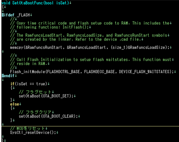
    By placing the entire API library in the .TI.ramfunc section, we have begun to see signs of a solution.

    We are currently executing a memcpy right before the FLASH operation function “setOtaBoot”, and we are verifying the process that stores all required functions in RAM.

    Could you please let us know whether it is possible to place the entire API library into the .TI.ramfunc section?

    MEMORY
    {
    PAGE 0 :  /* Program Memory */
              /* Memory (RAM/FLASH) blocks can be moved to PAGE1 for data allocation */
              /* BEGIN is used for the "boot to Flash" bootloader mode   */
    
    //   BEGIN           	: origin = 0x080000, length = 0x000002
       BEGIN           	: origin = 0x0B0000, length = 0x000002
       RAMM0           	: origin = 0x000123, length = 0x0002DD
       RAMD0           	: origin = 0x00B000, length = 0x000800
       RAMLS0          	: origin = 0x008000, length = 0x000800
       RAMLS1          	: origin = 0x008800, length = 0x000800
    //   RAMLS2      		: origin = 0x009000, length = 0x000800
       RAMGS14          : origin = 0x01A000, length = 0x001000     /* Only Available on F28379D, F28377D, F28375D devices. Remove line on other devices. */
       RAMGS15          : origin = 0x01B000, length = 0x000FF8     /* Only Available on F28379D, F28377D, F28375D devices. Remove line on other devices. */
    
    //   RAMGS15_RSVD     : origin = 0x01BFF8, length = 0x000008    /* Reserve and do not use for code as per the errata advisory "Memory: Prefetching Beyond Valid Memory" */
    
       RESET           	: origin = 0x3FFFC0, length = 0x000002
    
       /* Flash sectors */
    //   FLASHA           : origin = 0x080002, length = 0x001FFE	/* on-chip Flash */
    //   FLASHB           : origin = 0x082000, length = 0x002000	/* on-chip Flash */
    //   FLASHC           : origin = 0x084000, length = 0x002000	/* on-chip Flash */
    //   FLASHD           : origin = 0x086000, length = 0x002000	/* on-chip Flash */
    //   FLASHE           : origin = 0x088000, length = 0x008000	/* on-chip Flash */
    //   FLASHF           : origin = 0x090000, length = 0x008000	/* on-chip Flash */
    //   FLASHG           : origin = 0x098000, length = 0x008000	/* on-chip Flash */
    //   FLASHH           : origin = 0x0A0000, length = 0x008000	/* on-chip Flash */
    //   FLASHI           : origin = 0x0A8000, length = 0x008000	/* on-chip Flash */
       FLASHJ           : origin = 0x0B0002, length = 0x007F7E, fill = 0xffff	    /* on-chip Flash */
       FLASHJ_OTA_BOOT_FUNC : origin = 0x0B7F80, length = 0x000070, fill = 0xffff  /* on-chip Flash */
       FLASHJ_PRGINFO   : origin = 0x0B7FF0, length = 0x000010, fill = 0xffff	    /* on-chip Flash */
    
    //   FLASHK           : origin = 0x0B8000, length = 0x002000	/* on-chip Flash */
    //   FLASHL           : origin = 0x0BA000, length = 0x002000	/* on-chip Flash */
    //   FLASHM           : origin = 0x0BC000, length = 0x002000	/* on-chip Flash */
    //   FLASHN           : origin = 0x0BE000, length = 0x001FF0	/* on-chip Flash */
    
    //   FLASHN_RSVD     : origin = 0x0BFFF0, length = 0x000010    /* Reserve and do not use for code as per the errata advisory "Memory: Prefetching Beyond Valid Memory" */
    
    PAGE 1 : /* Data Memory */
             /* Memory (RAM/FLASH) blocks can be moved to PAGE0 for program allocation */
    
       BOOT_RSVD       : origin = 0x000002, length = 0x000121     /* Part of M0, BOOT rom will use this for stack */
       RAMM1           : origin = 0x000400, length = 0x0003F8     /* on-chip RAM block M1 */
    //   RAMM1_RSVD      : origin = 0x0007F8, length = 0x000008     /* Reserve and do not use for code as per the errata advisory "Memory: Prefetching Beyond Valid Memory" */
    //   RAMD1           : origin = 0x00B800, length = 0x000800
       RAMD1           : origin = 0x00B800, length = 0x000780
       RAMD1_REPRO_CRCINF : origin = 0x00BF80, length = 0x000080	/*各種CRC演算結果、ベリファイ結果保持領域*/
    
       RAMLS2      : origin = 0x009000, length = 0x000800
       RAMLS3      : origin = 0x009800, length = 0x000800
       RAMLS4      : origin = 0x00A000, length = 0x000800
       RAMLS5      : origin = 0x00A800, length = 0x000800
    
       RAMGS0      : origin = 0x00C000, length = 0x001000
       RAMGS1      : origin = 0x00D000, length = 0x001000
       RAMGS2      : origin = 0x00E000, length = 0x001000
       RAMGS3      : origin = 0x00F000, length = 0x001000
       RAMGS4      : origin = 0x010000, length = 0x001000
       RAMGS5      : origin = 0x011000, length = 0x001000
       RAMGS6      : origin = 0x012000, length = 0x001000
       RAMGS7      : origin = 0x013000, length = 0x001000
       RAMGS8      : origin = 0x014000, length = 0x001000
       RAMGS9      : origin = 0x015000, length = 0x001000
       RAMGS10     : origin = 0x016000, length = 0x001000
    
    //   RAMGS11     : origin = 0x017000, length = 0x000FF8   /* Uncomment for F28374D, F28376D devices */
    
    //   RAMGS11_RSVD : origin = 0x017FF8, length = 0x000008    /* Reserve and do not use for code as per the errata advisory "Memory: Prefetching Beyond Valid Memory" */
    
       RAMGS11     : origin = 0x017000, length = 0x001000     /* Only Available on F28379D, F28377D, F28375D devices. Remove line on other devices. */
       RAMGS12     : origin = 0x018000, length = 0x001000     /* Only Available on F28379D, F28377D, F28375D devices. Remove line on other devices. */
       RAMGS13     : origin = 0x019000, length = 0x001000     /* Only Available on F28379D, F28377D, F28375D devices. Remove line on other devices. */
    
       CPU2TOCPU1RAM   : origin = 0x03F800, length = 0x000400
       CPU1TOCPU2RAM   : origin = 0x03FC00, length = 0x000400
    }
    
    SECTIONS
    {
       /* Allocate program areas: */
       .cinit              : > FLASHJ      PAGE = 0, ALIGN(8)
       .text               : >> FLASHJ     PAGE = 0, ALIGN(8)
       codestart           : > BEGIN       PAGE = 0, ALIGN(8)
       OTA_BOOT_FUNC : > FLASHJ_OTA_BOOT_FUNC, PAGE = 0, ALIGN(8)
    
       PROGINF : > FLASHJ_PRGINFO, PAGE = 0, ALIGN(8)
    
       /* Allocate uninitalized data sections: */
       .stack              : > RAMM1       PAGE = 1
       .switch             : > FLASHJ      PAGE = 0, ALIGN(8)
       .reset              : > RESET,      PAGE = 0, TYPE = DSECT /* not used, */
    
    #if defined(__TI_EABI__)
       .init_array         : > FLASHJ,       PAGE = 0,       ALIGN(8)
       .bss                : > RAMLS3 | RAMLS4 | RAMLS5,       PAGE = 1
       .bss:output         : > RAMLS3 | RAMLS4,       PAGE = 0
       .bss:cio            : > RAMLS5,       PAGE = 1
       .data               : > RAMLS3 | RAMLS4 | RAMLS5,       PAGE = 1
       .sysmem             : > RAMLS2 | RAMLS5,       PAGE = 1
       /* Initalized sections go in Flash */
       .const              : > FLASHJ,       PAGE = 0,       ALIGN(8)
    #else
       .pinit              : > FLASHJ,       PAGE = 0,       ALIGN(8)
       .ebss               : >> RAMLS2 | RAMLS3 | RAMLS4 | RAMLS5 | RAMGS10 | RAMGS0 | RAMGS1,    PAGE = 1
       .esysmem            : > RAMLS2 | RAMLS5,       PAGE = 1
       .cio                : > RAMLS5,       PAGE = 1
       /* Initalized sections go in Flash */
       .econst             : >> FLASHJ      PAGE = 0, ALIGN(8)
    #endif
    
       Filter_RegsFile     : > RAMGS0,	   PAGE = 1
    
       SHARERAMGS0		: > RAMGS0,		PAGE = 1
       SHARERAMGS1		: > RAMGS1,		PAGE = 1
       SHARERAMGS2		: > RAMGS2,		PAGE = 1
       ramgs0           : > RAMGS0,     PAGE = 1
       ramgs1           : > RAMGS1,     PAGE = 1
    
    #ifdef __TI_COMPILER_VERSION__
        #if __TI_COMPILER_VERSION__ >= 15009000
            #if defined(__TI_EABI__)
                .TI.ramfunc : {} LOAD = FLASHJ,
                                     RUN = RAMLS0,
                                     LOAD_START(RamfuncsLoadStart),
                                     LOAD_SIZE(RamfuncsLoadSize),
                                     LOAD_END(RamfuncsLoadEnd),
                                     RUN_START(RamfuncsRunStart),
                                     RUN_SIZE(RamfuncsRunSize),
                                     RUN_END(RamfuncsRunEnd),
                                     PAGE = 0, ALIGN(8)
            #else
                .TI.ramfunc : {} LOAD = FLASHJ,
                                 RUN = RAMLS0,
                                 LOAD_START(_RamfuncsLoadStart),
                                 LOAD_SIZE(_RamfuncsLoadSize),
                                 LOAD_END(_RamfuncsLoadEnd),
                                 RUN_START(_RamfuncsRunStart),
                                 RUN_SIZE(_RamfuncsRunSize),
                                 RUN_END(_RamfuncsRunEnd),
                                 PAGE = 0, ALIGN(8)
            #endif
        #else
       ramfuncs            : LOAD = FLASHJ,
                             RUN = RAMLS0,
                             LOAD_START(_RamfuncsLoadStart),
                             LOAD_SIZE(_RamfuncsLoadSize),
                             LOAD_END(_RamfuncsLoadEnd),
                             RUN_START(_RamfuncsRunStart),
                             RUN_SIZE(_RamfuncsRunSize),
                             RUN_END(_RamfuncsRunEnd),
                             PAGE = 0, ALIGN(8)
        #endif
    
    #endif
       /* Allocate DMA-accessible RAM sections: */
       DMARAML7            : > RAMGS13,      PAGE = 1
       
       /* The following section definitions are required when using the IPC API Drivers */
        GROUP : > CPU1TOCPU2RAM, PAGE = 1
        {
            PUTBUFFER
            PUTWRITEIDX
            GETREADIDX
        }
    
        GROUP : > CPU2TOCPU1RAM, PAGE = 1
        {
            GETBUFFER :    TYPE = DSECT
            GETWRITEIDX :  TYPE = DSECT
            PUTREADIDX :   TYPE = DSECT
        }
    
       MSGRAM_CPU1_TO_CPU2 > CPU1TOCPU2RAM, type=NOINIT
       MSGRAM_CPU2_TO_CPU1 > CPU2TOCPU1RAM, type=NOINIT
       REPRO_RESULT_RAMD1 >  RAMD1_REPRO_CRCINF, type=NOINIT
    
       /* The following section definition are for SDFM examples */
       Filter1_RegsFile : > RAMGS1,	PAGE = 1, fill=0x1111
       Filter2_RegsFile : > RAMGS2,	PAGE = 1, fill=0x2222
       Filter3_RegsFile : > RAMGS3,	PAGE = 1, fill=0x3333
       Filter4_RegsFile : > RAMGS4,	PAGE = 1, fill=0x4444
       Difference_RegsFile : >RAMGS5, 	PAGE = 1, fill=0x3333
    }
    
    /*
    //===========================================================================
    // End of file.
    //===========================================================================
    */
    
    pcs_cpu1_repro.map.txt

    Best Regards,

    Ito

  • Hello Ito,

    Yes, it is possible. You can refer to this linker file in the C2000Ware SDK: c2000ware/device_support/f2837xd/examples/dual/flash_programming/cpu01/flash_programming_cpu1_FLASH.cmd.

    Best,

    Alex