This thread has been locked.

If you have a related question, please click the "Ask a related question" button in the top right corner. The newly created question will be automatically linked to this question.

TMS320C5535: The AD conversion values are offset and exhibit variation.

Genius 3215 points

Part Number: TMS320C5535

Hi All,

We are using pins GPAIN0–2 to monitor voltages such as 1.8V and the product’s battery level (4V–7V).

However, sometimes the battery level is displayed correctly, and sometimes it is not.
When checking the AD values from the DSP, we see cases where there is an offset of about 10 counts even though there is no input, and cases where there is both an offset and variation in the readings (also about 0–10 counts).
We are currently investigating the cause of this phenomenon.

Initially, we suspected a mounting defect, but X-ray inspection confirmed that there are no issues with the assembly.
Below is the schematic of the relevant section.
Do you see any mistakes in this circuit?
Also, have you encountered similar issues in the past?
If you have any suggestions on methods to investigate the root cause, please let us know.
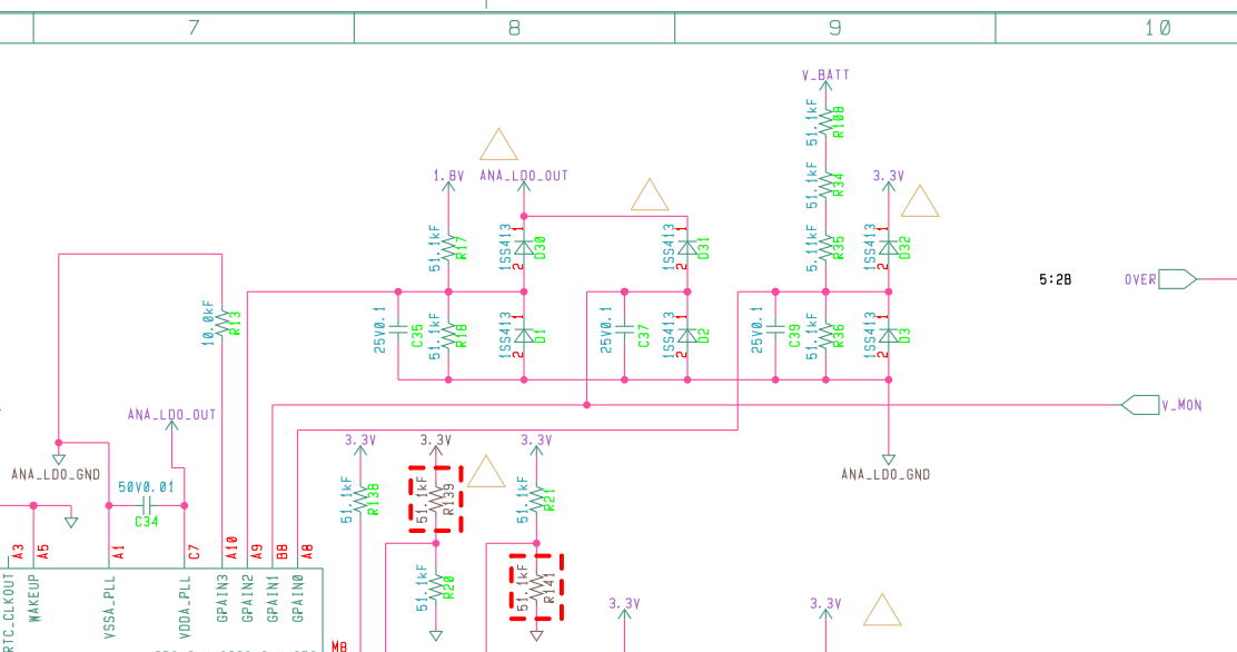
ADcircuit.png

Best Regards,

Ito

  • Hi Ito-san,

    What is the voltage range on V_MON?  Does it fall below 1.3V?  I don't see anything else from the schematic perspective that concerns me (as long as you are using the internal dividers on the 3.6V tolerant GPAIN0 to keep the voltage within range).

    What are the settings on the ADC configuration?  Are you using a 2MHz ADC internal conversion clock and delaying for at least 32 clock cycles?

    Can you provide a series of readings on a DC voltage that highlight the issue?

    How many devices are showing this issue?  Is it all devices tested or a subset?  How many devices tested are providing good data and how many are providing this shifted data?

    Thanks,
    Mike

  • Hi Mike,

    Thank you for your reply.

    We are reviewing the questions you submitted.

    The resistor values in the voltage divider are higher than recommended, so I’m a bit concerned.
    I believe high impedance is probably not ideal for a SAR ADC—do you have any thoughts on this?

    Best Regars,

    Ito

  • Ito-san,

    Yes, in general higher resistance values impact the ADC conversion by requiring longer sampling times to allow the signals to settle.  This is why I was asking about the configuration on the ADC.

    If the ADC is being used as maximum sample rate, then lowing the resistor values will likely help, however, keep in mind that the ANA_LDO can only drive a maximum of 4mA, so you need to keep the total current on this rail less than 4mA.

    Alternatively, you can try a longer ADC Conversion time by slowing down the ADC Clock or similar and see if the behavior improves or goes away.  This would be another indicator that the input is not sufficiently settling during the allocated conversion time.

    Thanks,
    Mike

  • Hi Mike,

    Thank you for your reply.

    If the ADC is being used as maximum sample rate, then lowing the resistor values will likely help, however, keep in mind that the ANA_LDO can only drive a maximum of 4mA, so you need to keep the total current on this rail less than 4mA.

    Is the interpretation of the total current on the rail correct as the total current at the pins GPAIN0–2?

    Best Regards,

    Ito

  • Ito-san,

    Is the interpretation of the total current on the rail correct as the total current at the pins GPAIN0–2?

    While the current on pins GPAIN0-2 is included in the total current calculation for ANA_LDO, the 4mA limit also includes everything else connected to ANA_LDO, such as VDDA_PLL (that I can see is connected in your schematic) and VDDA_ANA (not visible in the schematic shown to determine if it is sourced from ANA_LDO or somewhere else).

    According to the datasheet, VDDA_PLL typically pulls 0.7mA and VDDA_ANA pulls up to 1mA.  Assuming VDDA_ANA is also sourced in the design from ANA_LDO, then the total current draw allowed on the GPAIN circuitry is 2.3mA.  I know the primary voltage source for the voltage dividers on the GPAIN inputs is not ANA_LDO but a different supply.  This should keep the current draw here below 2.3mA.  But since I cannot see the rest of the schematic, I wanted to highlight that total system wide current draw on ANA_LDO output must be kept to less that 4mA.

    Also, please note that there is a requirement that the ANA_LDO has a 1uF capacitor.  I don't see this capacitor in the schematic (may just be out of this image), but want to confirm its presence.

    Thanks,
    Mike