Part Number: F29H859TU-Q1
Hello,
Could you please help clarifying the below points?
Figure 2-1 Device Reset Diagram in the device TRM revision A page 86 seems to imply that internally, PORESETn will keep the HSM and the CPU cores in reset if LPOST fails. Is that so? The diagrams in section 3.5.1 Device Boot Flow show otherwise. How should LPOST in the way of PORESETn be interpreted in fig. 2-1? Assuming LPOST fails, what is the SoC expected to do? If the HSM or CPU1 are supposed to handle an LPOST failure, how about an LPOST failure that's actually due to an HSM or CPU1 logic failure?
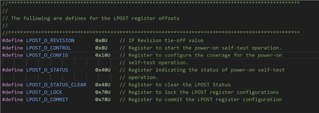
The LPOST status bits do not seem to be documented in the TRM. One has to look for their definition in the SDK (source\bitfields\hwbf_lpost.h). I could not spot the address of this register either: the SDK file source\driverlib\inc\hw_lpost.h lists the LPOST register offsets, but the base address of the LPOST registers block is nowhere to be found—SDK, datasheet or TRM. Are the LPOST registers fully defined in a document, and what are their base address?
TRM section 3.7.11 BootROM Timing lists some timings for the execution of LPOST and MPOST, but without specifying the LPOST coverage nor specifying the PLL setting. Could you please provide the run-time for the different LPOST coverages and tell the PLL setting used in the table? Also, assuming one would want to run LPOST/MPOST using the PLL, why one would select a PLL frequency other than the highest one possible so to shorten the execution time of the tests?
We have similar questions for MPOST: where are the MPOST status registers located and described? And how is one supposed to handle an MPOST failure?
Thank you.
Best regards,
François.