This thread has been locked.

If you have a related question, please click the "Ask a related question" button in the top right corner. The newly created question will be automatically linked to this question.

TMS320F28P559SJ-Q1: CMPSS with Ramp - Unintentional Blanking Area

Part Number: TMS320F28P559SJ-Q1
Other Parts Discussed in Thread: TMDSCNCD28P55X

Dear Expert.


I have problem on using CMPSS.

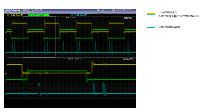
I watching CTRIPOUT, it is raw output of COMP, and unfiltered.


And I try to using ramp generetor as Compinput minus.

Of course, it should work as described above.

But, Comp input plus becomes higher, CompOut works as unexpected.


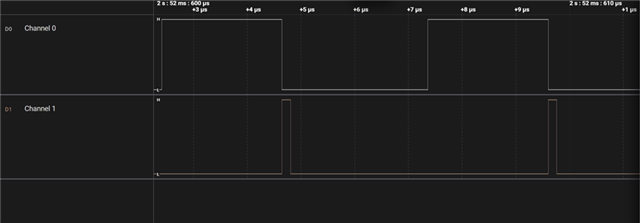
Wave is below.

It doesn't applied any Blanking, but there is unexpected Non-responsive Area.

1. Why is this occur?

2. How should be fixed?


Best regards.

  • Hi Ryushi,
    I am going through the query, will get back to you in a couple of days. Meanwhile, it would be really helpful if you can share details regarding configuration. If possible, can you share your Syscfg file?
    And Can you provide details regarding application? 
    Thanks,
    Praneeth

  • Dear Praneeth.

    Thank for your response.

    I'm sorry, but due to confidential information, we are unable to provide the file at this time(It is under discussion.).

    Another information is found.

    We stop Main PWM_A,B (in above waveform) output by applying too long deadtime(but other ePWM functions are working), and unexpected behavior of Compout is not happen.

    So we suspect that the PWM output is affecting the behavior of the comparator.

    Best regards.

  • Ryushi, 

    Thanks for the reply. I have following questions. 
    1. And you mentioned that you applied longer deadtime for PWM A and B, this behavior of COMPUT is not happening. Can you share a scope shot of this?
    2. I can see the CMPSS out is not tripping the ePWM pulse? So is it supposed to be like that? Or if possible, Can I know what the COMPTOUT is supposed to do?

    Thanks,
    Praneeth

  • Dear Praneeth

    >Q1

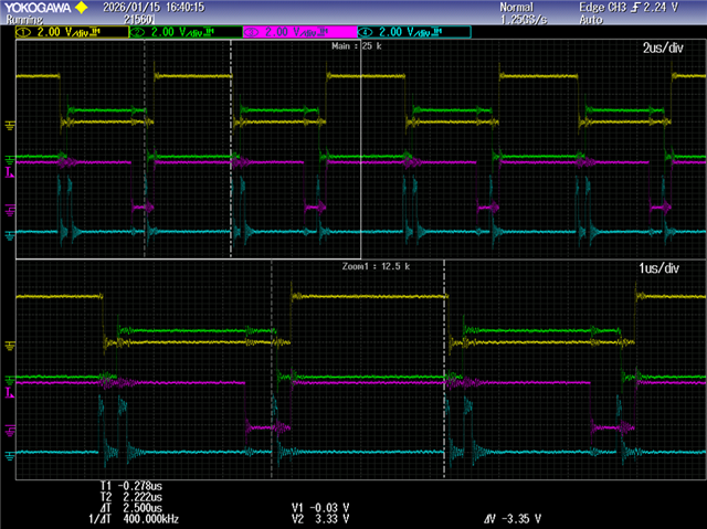
    First, unexpected behavior is below.

    (This shot is by overwriting mode.

    Today, splitting in same time is not found, but Non-responsive Area is found.)

    In the same condition, without software stop PWM A, B by long deadtime.

    Scope shot is below.

    >Q2

    That's right. There is another pair of waveform controlled by the CMPSS.(we call them sub PWM C,D)

    And that wave is stopping as main PWM too.

    sub PWM is doubtful too, but logicaly, Trip of CMPSS changes sub PWM output on/off, so I think that sub PWM output on/off is not  cause of wrong Comp out(especially, first output of splitting).

    Best regards.

  • Ryushi,

    Thank you for sharing the information. Even without main PWMs, tripping occurs? So the tripping is because of some voltage or current which is independent of main PWMS. Am I right? I am asking this because, if switching is happening, most probable cause would be the noise due to this switching. If this is the case, I would recommend to use latch in ePWM module, if not used already. 


    Thanks
    Praneeth

  • We have additional experiment.

    Condition is main PWM stop but sub PWM remain.

    And it occured spilitting, but Non-responsive Area is not occured.

    Best regards.

  • Dear Praneeth

    Thank for your response.

    These experiments are on test board and just stop outputing, so CMPSS should works ordinaly, and Tripping too.

    PWM TimeBase unit occures SYNCPER, SYNCPER resets CMPSS and Ramp, CMPSS occurs sub PWM Tripping.

    sub PWM switching noise may occurs second COMPOUT (above newest scope says.). And it is not serious problem because we are already using digital filter latch, you recomended.

    But I wonder why Non-Responsible area is made (by main PWM). And this is serious problem.

    Best regards.


  • Ryushi,
    Please correct me if I am wrong. 
    Falling edge of yellow and green pulses should have CMPSSOUT pulse. But during experiment, you are observing pulses after the falling edge.
    Am I correctly understanding the issue?
    Thanks
    Praneeth 

  • Dear Praneeth

    Sorry if you say about this scope,

    We have additional experiment.

    yellow and green wave in this scope are not main PWM(because they are surpressed), but sub PWM. sub PWM does not generate SYNCPER, but falling by CMPSSOUT. So falling edge and CMPSSOUT are same timing. And it is not a problem.

    It seems main PWM rising edge(or fallng edge?) make CMPSS wrong behavior, that is making too fast signal.

    Best regards.

  • Ryushi,
    Thank you for explaining patiently. It is very useful. CMPSS ramp will start decrementing or incrementing at the SYNCPER signal. But the pulse will be seen only when the CMPSS reference is equal to ramp generator value. My next question is, why main PWM edge is being taken as reference for CMPSS out signal? CMPSS out will have a pulse when Ramp generator equal to reference value, but not at the rising/falling edge of the main PWM. 
    Please correct me if I am wrong anywhere.
    Thanks
    Praneeth

  • Dear Praneeth

    This problem occurs only when Comp Input+ voltage(=reference value) is near to Ramp MAX. So we setting as it in scopes.

    If input near to Ramp MAX and if Ramp reset falling egdes of main PWM, CTRIPOUT should be near to fallng/rising edges, isn't it?

    In actual application, Comp Input+ changes dynamically.

    Best regards.

  • Ryushi,
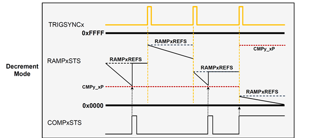
    Thanks again for explanation. From what I have understood, your input value is near to RAMP reference MAX. And your falling edge is set as reset for CMPSS, so this is SYNCPER signal. This situation is described in the TRM. 

    If your input is very near to ramp max, your pulse will be very close to falling edge of the pulse. You will see Comp out pulse to be coinciding with the falling edge only when input value is  equal to or more than Ramp max value, when falling edge is detected. Can you check if this is the case with your sampled input signal?
    And also, have you applied any delay in your syscfg configuration? Because ramp generator would not start decrementing until the number of cycles mentioned in this field have passed.

    Thanks,
    Praneeth

  • Dear Praneeth.

    Thank for your response.

    >TRM

    Yes, this image can describe our setting.

    >Can you check if this is the case with your sampled input signal?

    I couldn't show scope now, but I tried it.

    If input value(voltage) is bigger than Ramp MAX, CTRIPOUT keep high and don't goto low.

    Just for your information, this problem occur near to rising edge of main PWM.

    The following is my guess.

    >syscfg

    I didn't delay value.

    Best regards.

  • Ryushi,

    Why is this pulse expected? 
    Thanks
    Praneeth

  • Dear Praneeth

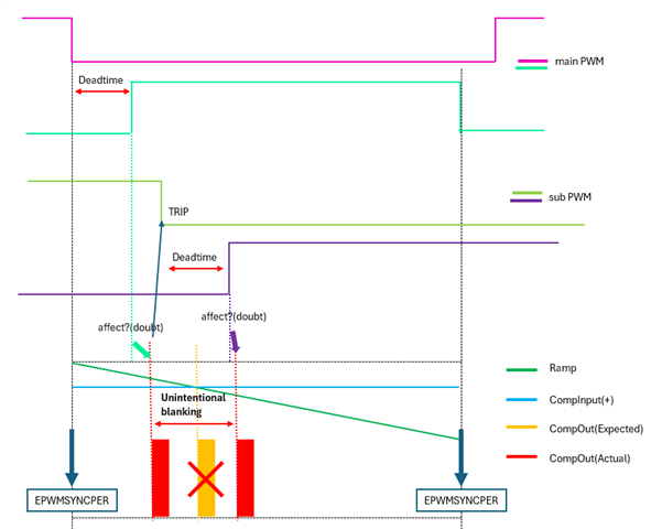
    I'm sorry that was miss copied object.. 

    I fixed it and add sub PWM affecting doubt too.

    Best regard.

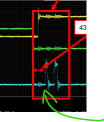
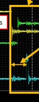
  • Ryushi,
    Thanks for the clarification. Can you please indicate the unintentional blanking time in this picture itself, to avoid confusion? 
    Thanks,
    Praneeth

  • Dear Praneeth

    Thank you for your responcse.

    I add unintentional blanking.

    Best regard.

  • Ryushi,
    Thanks for the picture. As you have not used blanking, filter and Delay, I am confident that second pulse is due to the sensed signal having noise on it, and I do not think blanking is happening there. I would recommend to check the sensed signal by probing it.
    Thanks
    Praneeth

  • Dear Praneeth

    > I would recommend to check the sensed signal by probing it

    Input signal is not affected by noise, because this problem is occuring in both target hardware and TMDSCNCD28P55X evaboard too.

    Both VDDA and VDDIO remain constant value when problem occur.

    So, I 'm worried that there may be noise inside the chip, and it affecting DAC or CMPSS.

    Best regard.

  • Ryushi,

    As it is happening in Launchpad as well, I will try to capture the pulse scope shot from my end, I will get back to you in a couple of days. Meanwhile, Can you try applying hysteresis and digital filter and try again? 
    Thanks,
    Praneeth

  • Hi Ryushi,
    Below is the scope shot of PWM pulse and the CTRIP pulse. I did not use hysteresis and digital filter

    Please try with hysteresis and digital filter, this should negate the effect of noise whatever the source may be. If the problem still persists, I am afraid I need to see the sensed signal for better debugging. 
    Thanks 
    Praneeth

  • Dear Praneeth

    I'm sorry that my response is late.

    We check input of TMDSCNCD28P55X and the input was very noisy(+- 0.5[V]).

    We use TMDSCNCD28P55X rev.A, and its sch shows that it has input filter.


    But our board is not implemented Cxx capacitors.

    Why hasn't it been implemented?

    Best regard.

  • Ryushi,
    In the design files that are provided, altium project file is included. In that project two variants are there. One is with the required circuitry only. This is the variant that is used for fabrication. This is the reason why your board does not have these filter capacitors. 

    In the information guide , this is mentioned. They are not populated by default.  

    Thanks
    Praneeth