Part Number: LAUNCHXL-F280049C
Hello E2E Experts,

This thread has been locked.
If you have a related question, please click the "Ask a related question" button in the top right corner. The newly created question will be automatically linked to this question.
Part Number: LAUNCHXL-F280049C
Hello E2E Experts,

Hello Wang,
Bit timing setup shows the baud rate at 125Kbps. Can you provide more details on the problem/setup:
1.) What is the main source of device clock (internal oscillator or external clock) and what is SYSCLK configured to? What is the clock configuration?
2.) Error is coming from transmission that is causing the node to go bus off. Can you provide CAN frame waveform when node starts transmitting frames?
Thanks,
Joseph
yes we can use 125kbps
1 we use external clock
//###########################################################################
//
// FILE: f28004x_sysctrl.c
//
// TITLE: f28004x Device System Control Initialization & Support Functions.
//
// DESCRIPTION: Example initialization of system resources.
//
//###########################################################################
//
//
// $Copyright:
// Copyright (C) 2022 Texas Instruments Incorporated - http://www.ti.com/
//
// Redistribution and use in source and binary forms, with or without
// modification, are permitted provided that the following conditions
// are met:
//
// Redistributions of source code must retain the above copyright
// notice, this list of conditions and the following disclaimer.
//
// Redistributions in binary form must reproduce the above copyright
// notice, this list of conditions and the following disclaimer in the
// documentation and/or other materials provided with the
// distribution.
//
// Neither the name of Texas Instruments Incorporated nor the names of
// its contributors may be used to endorse or promote products derived
// from this software without specific prior written permission.
//
// THIS SOFTWARE IS PROVIDED BY THE COPYRIGHT HOLDERS AND CONTRIBUTORS
// "AS IS" AND ANY EXPRESS OR IMPLIED WARRANTIES, INCLUDING, BUT NOT
// LIMITED TO, THE IMPLIED WARRANTIES OF MERCHANTABILITY AND FITNESS FOR
// A PARTICULAR PURPOSE ARE DISCLAIMED. IN NO EVENT SHALL THE COPYRIGHT
// OWNER OR CONTRIBUTORS BE LIABLE FOR ANY DIRECT, INDIRECT, INCIDENTAL,
// SPECIAL, EXEMPLARY, OR CONSEQUENTIAL DAMAGES (INCLUDING, BUT NOT
// LIMITED TO, PROCUREMENT OF SUBSTITUTE GOODS OR SERVICES; LOSS OF USE,
// DATA, OR PROFITS; OR BUSINESS INTERRUPTION) HOWEVER CAUSED AND ON ANY
// THEORY OF LIABILITY, WHETHER IN CONTRACT, STRICT LIABILITY, OR TORT
// (INCLUDING NEGLIGENCE OR OTHERWISE) ARISING IN ANY WAY OUT OF THE USE
// OF THIS SOFTWARE, EVEN IF ADVISED OF THE POSSIBILITY OF SUCH DAMAGE.
// $
//###########################################################################
//
// Included Files
//
#include "f28004x_device.h" // Headerfile Include File
#include "f28004x_examples.h" // Examples Include File
#include "device.h"
#ifdef __cplusplus
using std::memcpy;
#endif
//
// Functions that will be run from RAM need to be assigned to
// a different section. This section will then be mapped to a load and
// run address using the linker cmd file.
//
// *IMPORTANT*
// IF RUNNING FROM FLASH, PLEASE COPY OVER THE SECTION ".TI.ramfunc" FROM FLASH
// TO RAM PRIOR TO CALLING InitSysCtrl(). THIS PREVENTS THE MCU FROM THROWING
// AN EXCEPTION WHEN A CALL TO DELAY_US() IS MADE.
//
#ifndef __cplusplus
#pragma CODE_SECTION(InitFlash, ".TI.ramfunc");
#pragma CODE_SECTION(FlashOff, ".TI.ramfunc");
#endif
//
// The following values are used to validate PLL Frequency using DCC
//
#define PLL_RETRIES 100
#define PLL_LOCK_TIMEOUT 2000
#define DCC_COUNTER0_WINDOW 100
//
// Macro used for adding delay between 2 consecutive writes to CLKSRCCTL1
// register.
// Delay = 300 NOPs
//
#define SYSCTRL_CLKSRCCTL1_DELAY asm(" RPT #250 || NOP \n RPT #50 || NOP")
#define _FLASH
//
// InitSysCtrl - Initialization of system resources.
//
void
InitSysCtrl(void)
{
//
// Disable the watchdog
//
DisableDog();
#ifdef _FLASH
//
// Copy time critical code and Flash setup code to RAM
// This includes the following functions: InitFlash();
// The RamfuncsLoadStart, RamfuncsLoadSize, and RamfuncsRunStart
// symbols are created by the linker. Refer to the device .cmd file.
//
memcpy(&RamfuncsRunStart, &RamfuncsLoadStart, (size_t)&RamfuncsLoadSize);
//
// Call Flash Initialization to setup flash waitstates
// This function must reside in RAM
//
InitFlash();
#endif
//
// PLLSYSCLK = (XTAL_OSC) * (IMULT + FMULT) / (PLLSYSCLKDIV)
//
#ifdef _LAUNCHXL_F280049C
InitSysPll(XTAL_OSC,IMULT_10,FMULT_0,PLLCLK_BY_2);//崔幔XTAL_OSC
#else
InitSysPll(XTAL_OSC_SE,IMULT_10,FMULT_0,PLLCLK_BY_2);//崔幔XTAL_OSC
#endif
#ifndef _FLASH
//
// Call Device_cal function when run using debugger
// This function is called as part of the Boot code. The function is called
// in the InitSysCtrl function since during debug time resets, the boot code
// will not be executed and the gel script will reinitialize all the
// registers and the calibrated values will be lost.
//
Device_cal();
#endif
//
// Turn on all peripherals
//
InitPeripheralClocks();
}
//
// InitPeripheralClocks - This function initializes the clocks for the
// peripherals. Note: In order to reduce power consumption, turn off the
// clocks to any peripheral that is not specified for your part-number or is
// not used in the application
//
void
InitPeripheralClocks()
{
EALLOW;
ClkCfgRegs.LOSPCP.all= 0x0002;//崔幔 低速时钟25M 100M\2*N
CpuSysRegs.PCLKCR0.bit.CLA1 = 1;
CpuSysRegs.PCLKCR0.bit.DMA = 1;
CpuSysRegs.PCLKCR0.bit.CPUTIMER0 = 1;
CpuSysRegs.PCLKCR0.bit.CPUTIMER1 = 1;
CpuSysRegs.PCLKCR0.bit.CPUTIMER2 = 1;
CpuSysRegs.PCLKCR0.bit.HRPWM = 1;
// CpuSysRegs.PCLKCR0.bit.TBCLKSYNC = 1;
CpuSysRegs.PCLKCR2.bit.EPWM1 = 1;
CpuSysRegs.PCLKCR2.bit.EPWM2 = 1;
CpuSysRegs.PCLKCR2.bit.EPWM3 = 1;
CpuSysRegs.PCLKCR2.bit.EPWM4 = 1;
CpuSysRegs.PCLKCR2.bit.EPWM5 = 1;
CpuSysRegs.PCLKCR2.bit.EPWM6 = 1;
CpuSysRegs.PCLKCR2.bit.EPWM7 = 1;
CpuSysRegs.PCLKCR2.bit.EPWM8 = 1;
CpuSysRegs.PCLKCR3.bit.ECAP1 = 1;
CpuSysRegs.PCLKCR3.bit.ECAP2 = 1;
CpuSysRegs.PCLKCR3.bit.ECAP3 = 1;
CpuSysRegs.PCLKCR3.bit.ECAP4 = 1;
CpuSysRegs.PCLKCR3.bit.ECAP5 = 1;
CpuSysRegs.PCLKCR3.bit.ECAP6 = 1;
CpuSysRegs.PCLKCR3.bit.ECAP7 = 1;
CpuSysRegs.PCLKCR4.bit.EQEP1 = 1;
CpuSysRegs.PCLKCR4.bit.EQEP2 = 1;
CpuSysRegs.PCLKCR6.bit.SD1 = 1;
CpuSysRegs.PCLKCR7.bit.SCI_A = 1;
CpuSysRegs.PCLKCR7.bit.SCI_B = 1;
CpuSysRegs.PCLKCR8.bit.SPI_A = 1;
CpuSysRegs.PCLKCR8.bit.SPI_B = 1;
CpuSysRegs.PCLKCR9.bit.I2C_A = 1;
CpuSysRegs.PCLKCR10.bit.CAN_A = 1;
CpuSysRegs.PCLKCR10.bit.CAN_B = 1;
CpuSysRegs.PCLKCR13.bit.ADC_A = 1;
CpuSysRegs.PCLKCR13.bit.ADC_B = 1;
CpuSysRegs.PCLKCR13.bit.ADC_C = 1;
CpuSysRegs.PCLKCR14.bit.CMPSS1 = 1;
CpuSysRegs.PCLKCR14.bit.CMPSS2 = 1;
CpuSysRegs.PCLKCR14.bit.CMPSS3 = 1;
CpuSysRegs.PCLKCR14.bit.CMPSS4 = 1;
CpuSysRegs.PCLKCR14.bit.CMPSS5 = 1;
CpuSysRegs.PCLKCR14.bit.CMPSS6 = 1;
CpuSysRegs.PCLKCR14.bit.CMPSS7 = 1;
CpuSysRegs.PCLKCR15.bit.PGA1 = 1;
CpuSysRegs.PCLKCR15.bit.PGA2 = 1;
CpuSysRegs.PCLKCR15.bit.PGA3 = 1;
CpuSysRegs.PCLKCR15.bit.PGA4 = 1;
CpuSysRegs.PCLKCR15.bit.PGA5 = 1;
CpuSysRegs.PCLKCR15.bit.PGA6 = 1;
CpuSysRegs.PCLKCR15.bit.PGA7 = 1;
CpuSysRegs.PCLKCR18.bit.FSIRX_A = 1;
CpuSysRegs.PCLKCR18.bit.FSITX_A = 1;
CpuSysRegs.PCLKCR16.bit.DAC_A = 1;
CpuSysRegs.PCLKCR16.bit.DAC_B = 1;
CpuSysRegs.PCLKCR19.bit.LIN_A = 1;
CpuSysRegs.PCLKCR20.bit.PMBUS_A = 1;
CpuSysRegs.PCLKCR21.bit.DCC_0 = 1;
EDIS;
}
//
// DisablePeripheralClocks -
//
void
DisablePeripheralClocks()
{
EALLOW;
CpuSysRegs.PCLKCR0.all = 0;
CpuSysRegs.PCLKCR2.all = 0;
CpuSysRegs.PCLKCR3.all = 0;
CpuSysRegs.PCLKCR4.all = 0;
CpuSysRegs.PCLKCR6.all = 0;
CpuSysRegs.PCLKCR7.all = 0;
CpuSysRegs.PCLKCR8.all = 0;
CpuSysRegs.PCLKCR9.all = 0;
CpuSysRegs.PCLKCR10.all = 0;
CpuSysRegs.PCLKCR13.all = 0;
CpuSysRegs.PCLKCR14.all = 0;
CpuSysRegs.PCLKCR15.all = 0;
CpuSysRegs.PCLKCR16.all = 0;
CpuSysRegs.PCLKCR18.all = 0;
CpuSysRegs.PCLKCR19.all = 0;
CpuSysRegs.PCLKCR20.all = 0;
CpuSysRegs.PCLKCR21.all = 0;
EDIS;
}
//
// InitFlash - This function initializes the Flash Control registers
// CAUTION
// This function MUST be executed out of RAM. Executing it
// out of OTP/Flash will yield unpredictable results
//
#ifdef __cplusplus
#pragma CODE_SECTION(".TI.ramfunc");
#endif
void
InitFlash(void)
{
EALLOW;
//
// At reset bank and pump are in sleep
// A Flash access will power up the bank and pump automatically
//
// Power up Flash bank and pump and this also sets the fall back mode of
// flash and pump as active
//
Flash0CtrlRegs.FPAC1.bit.PMPPWR = 0x1;
Flash0CtrlRegs.FBFALLBACK.bit.BNKPWR0 = 0x3;
Flash0CtrlRegs.FBFALLBACK.bit.BNKPWR1 = 0x3;
//
// Disable Cache and prefetch mechanism before changing wait states
//
Flash0CtrlRegs.FRD_INTF_CTRL.bit.DATA_CACHE_EN = 0;
Flash0CtrlRegs.FRD_INTF_CTRL.bit.PREFETCH_EN = 0;
//
// Set waitstates according to frequency
// CAUTION
// Minimum waitstates required for the flash operating
// at a given CPU rate must be characterized by TI.
// Refer to the datasheet for the latest information.
//
#if CPU_FRQ_100MHZ
if((ClkCfgRegs.CLKSRCCTL1.bit.OSCCLKSRCSEL == 0x0) ||
(ClkCfgRegs.CLKSRCCTL1.bit.OSCCLKSRCSEL == 0x2) ||
(ClkCfgRegs.CLKSRCCTL1.bit.OSCCLKSRCSEL == 0x3))
{
Flash0CtrlRegs.FRDCNTL.bit.RWAIT = 0x5;
}
else
{
Flash0CtrlRegs.FRDCNTL.bit.RWAIT = 0x4;
}
#endif
//
// Enable Cache and prefetch mechanism to improve performance
// of code executed from Flash.
//
Flash0CtrlRegs.FRD_INTF_CTRL.bit.DATA_CACHE_EN = 1;
Flash0CtrlRegs.FRD_INTF_CTRL.bit.PREFETCH_EN = 1;
//
// At reset, ECC is enabled. If it is disabled by application software
// and if application again wants to enable ECC
//
Flash0EccRegs.ECC_ENABLE.bit.ENABLE = 0xA;
EDIS;
//
// Force a pipeline flush to ensure that the write to
// the last register configured occurs before returning.
//
__asm(" RPT #7 || NOP");
}
//
// FlashOff - This function powers down the flash
// CAUTION
// This function MUST be executed out of RAM. Executing it
// out of OTP/Flash will yield unpredictable results.
// Note: a flash access after the flash pump and banks are powered down will
// wake the pump and bank
//
#ifdef __cplusplus
#pragma CODE_SECTION(".TI.ramfunc");
#endif
void
FlashOff(void)
{
EALLOW;
//
// Configure the fallback power mode as sleep
//
Flash0CtrlRegs.FBFALLBACK.bit.BNKPWR0 = 0;
Flash0CtrlRegs.FBFALLBACK.bit.BNKPWR1 = 0;
//
// Configure the fallback power mode as sleep
//
Flash0CtrlRegs.FPAC1.bit.PMPPWR = 0;
EDIS;
}
//
// ServiceDog - This function resets the watchdog timer.
// Enable this function for using ServiceDog in the application
//
void
ServiceDog(void)
{
EALLOW;
WdRegs.WDKEY.bit.WDKEY = 0x0055;
WdRegs.WDKEY.bit.WDKEY = 0x00AA;
EDIS;
}
//
// DisableDog - This function disables the watchdog timer.
//
void
DisableDog(void)
{
volatile Uint16 temp;
EALLOW;
//
// Grab the clock config so we don't clobber it
//
temp = WdRegs.WDCR.all & 0x0007;
WdRegs.WDCR.all = 0x0068 | temp;
EDIS;
}
void EnableDog(void)
{
EALLOW;
WdRegs.WDCR.all = 0x002FU;
EDIS;
}
//
// InitPll - This function initializes the PLL registers.
//
// Note: This function uses the DCC to check that the PLLRAWCLK is running at
// the expected rate. If you are using the DCC, you must back up its
// configuration before calling this function and restore it afterward.
//
void
InitSysPll(Uint16 clock_source, Uint16 imult, Uint16 fmult, Uint16 divsel)
{
Uint32 timeout, retries, temp_syspllmult, pllLockStatus;
bool status;
if(((clock_source & 0x3) == ClkCfgRegs.CLKSRCCTL1.bit.OSCCLKSRCSEL) &&
(((clock_source & 0x4) >> 2) == ClkCfgRegs.XTALCR.bit.SE) &&
(imult == ClkCfgRegs.SYSPLLMULT.bit.IMULT) &&
(fmult == ClkCfgRegs.SYSPLLMULT.bit.FMULT) &&
(divsel == ClkCfgRegs.SYSCLKDIVSEL.bit.PLLSYSCLKDIV))
{
//
// Everything is set as required, so just return
//
return;
}
if(((clock_source & 0x3) != ClkCfgRegs.CLKSRCCTL1.bit.OSCCLKSRCSEL) ||
(((clock_source & 0x4) >> 2) != ClkCfgRegs.XTALCR.bit.SE))
{
switch (clock_source)
{
case INT_OSC1:
SysIntOsc1Sel();
break;
case INT_OSC2:
SysIntOsc2Sel();
break;
case XTAL_OSC:
SysXtalOscSel();
break;
case XTAL_OSC_SE:
SysXtalOscSESel();
break;
}
}
EALLOW;
//
// First modify the PLL multipliers
//
if(imult != ClkCfgRegs.SYSPLLMULT.bit.IMULT ||
fmult != ClkCfgRegs.SYSPLLMULT.bit.FMULT)
{
//
// Bypass PLL and set dividers to /1
//
ClkCfgRegs.SYSPLLCTL1.bit.PLLCLKEN = 0;
//
// Delay of at least 60 OSCCLK cycles required post PLL bypass
//
asm(" RPT #60 || NOP");
ClkCfgRegs.SYSCLKDIVSEL.bit.PLLSYSCLKDIV = 0;
//
// Evaluate PLL multipliers
//
temp_syspllmult = ((fmult << 8U) | imult);
//
// Loop to retry locking the PLL should the DCC module indicate
// that it was not successful.
//
for(retries = 0; (retries < PLL_RETRIES); retries++)
{
EALLOW;
//
// Disable SYSPLL (Turn off PLL)
//
ClkCfgRegs.SYSPLLCTL1.bit.PLLEN = 0;
//
// Atleast 60 cycle delay between powerdown to powerup
//
asm(" RPT #60 || NOP");
//
// Program PLL multipliers
//
ClkCfgRegs.SYSPLLMULT.all = temp_syspllmult;
//
// Enable SYSPLL
//
ClkCfgRegs.SYSPLLCTL1.bit.PLLEN = 1;
timeout = PLL_LOCK_TIMEOUT;
pllLockStatus = ClkCfgRegs.SYSPLLSTS.bit.LOCKS;
//
// Wait for the SYSPLL lock
//
while((pllLockStatus != 1) && (timeout != 0U))
{
pllLockStatus = ClkCfgRegs.SYSPLLSTS.bit.LOCKS;
timeout--;
}
EDIS;
status = IsPLLValid(clock_source, imult, fmult);
//
// Check DCC Status, if no error break the loop
//
if(status)
{
break;
}
}
}
else
{
status = true;
}
if(status)
{
EALLOW;
//
// Set divider to produce slower output frequency to limit current increase
//
if(divsel != PLLCLK_BY_126)
{
ClkCfgRegs.SYSCLKDIVSEL.bit.PLLSYSCLKDIV = divsel + 1;
}
else
{
ClkCfgRegs.SYSCLKDIVSEL.bit.PLLSYSCLKDIV = divsel;
}
//
// Enable PLLSYSCLK is fed from system PLL clock
//
ClkCfgRegs.SYSPLLCTL1.bit.PLLCLKEN = 1;
//
// Small 100 cycle delay
//
asm(" RPT #100 || NOP");
//
// Set the divider to user value
//
ClkCfgRegs.SYSCLKDIVSEL.bit.PLLSYSCLKDIV = divsel;
EDIS;
}
}
//
// CsmUnlock - This function unlocks the CSM. User must replace 0xFFFF's with
// current password for the DSP.
//
Uint16
CsmUnlock()
{
//
// Write to the key registers to unlock the device. The 0x0FFFFFFFF's
// are dummmy passwords. User should replace them with the correct password
// for the DSP.
// Note: F28004x has default password keys which are not all 0xFFFFFFFF.
// See DCSM chapter of Technical Reference Manual for default passwords.
EALLOW;
DcsmBank0Z1Regs.Z1_CSMKEY0 = 0xFFFFFFFF;
DcsmBank0Z1Regs.Z1_CSMKEY1 = 0xFFFFFFFF;
DcsmBank0Z1Regs.Z1_CSMKEY2 = 0xFFFFFFFF;
DcsmBank0Z1Regs.Z1_CSMKEY3 = 0xFFFFFFFF;
DcsmBank0Z2Regs.Z2_CSMKEY0 = 0xFFFFFFFF;
DcsmBank0Z2Regs.Z2_CSMKEY1 = 0xFFFFFFFF;
DcsmBank0Z2Regs.Z2_CSMKEY2 = 0xFFFFFFFF;
DcsmBank0Z2Regs.Z2_CSMKEY3 = 0xFFFFFFFF;
EDIS;
return 0;
}
//
// SysIntOsc1Sel - This function switches to Internal Oscillator 1 and turns
// off all other clock sources to minimize power consumption
//
void
SysIntOsc1Sel (void)
{
EALLOW;
ClkCfgRegs.CLKSRCCTL1.bit.OSCCLKSRCSEL = 2; // Clk Src = INTOSC1
ClkCfgRegs.XTALCR.bit.OSCOFF=1; // Turn off XTALOSC
EDIS;
}
//
// SysIntOsc2Sel - This function switches to Internal oscillator 2 from
// External Oscillator and turns off all other clock sources to minimize
// power consumption
// NOTE: If there is no external clock connection, when switching from
// INTOSC1 to INTOSC2, EXTOSC and XLCKIN must be turned OFF prior
// to switching to internal oscillator 1
//
void
SysIntOsc2Sel (void)
{
EALLOW;
ClkCfgRegs.CLKSRCCTL1.bit.INTOSC2OFF=0; // Turn on INTOSC2
SYSCTRL_CLKSRCCTL1_DELAY;
ClkCfgRegs.CLKSRCCTL1.bit.OSCCLKSRCSEL = 0; // Clk Src = INTOSC2
ClkCfgRegs.XTALCR.bit.OSCOFF=1; // Turn off XTALOSC
EDIS;
}
//
// PollX1Counter - Clear the X1CNT counter and then wait for it to saturate
// four times.
//
static void
PollX1Counter(void)
{
Uint16 loopCount = 0;
//
// Delay for 1 ms while the XTAL powers up
//
// 2000 loops, 5 cycles per loop + 9 cycles overhead = 10009 cycles
//
F28x_usDelay(2000);
//
// Clear and saturate X1CNT 4 times to guarantee operation
//
do
{
//
// Keep clearing the counter until it is no longer saturated
//
while(ClkCfgRegs.X1CNT.all > 0x1FF)
{
ClkCfgRegs.X1CNT.bit.CLR = 1;
}
//
// Wait for the X1 clock to saturate
//
while(ClkCfgRegs.X1CNT.all != 0x3FFU)
{
;
}
//
// Increment the counter
//
loopCount++;
}while(loopCount < 4);
}
//
// SysXtalOscSel - This function switches to External CRYSTAL oscillator and
// turns off all other clock sources to minimize power consumption. This option
// may not be available on all device packages
//
void
SysXtalOscSel (void)
{
EALLOW;
ClkCfgRegs.XTALCR.bit.OSCOFF = 0; // Turn on XTALOSC
ClkCfgRegs.XTALCR.bit.SE = 0; // Select crystal mode
EDIS;
//
// Wait for the X1 clock to saturate
//
PollX1Counter();
//
// Select XTAL as the oscillator source
//
EALLOW;
ClkCfgRegs.CLKSRCCTL1.bit.OSCCLKSRCSEL = 1;
EDIS;
//
// If a missing clock failure was detected, try waiting for the X1 counter
// to saturate again. Consider modifying this code to add a 10ms timeout.
//
while(ClkCfgRegs.MCDCR.bit.MCLKSTS != 0)
{
EALLOW;
ClkCfgRegs.MCDCR.bit.MCLKCLR = 1;
EDIS;
//
// Wait for the X1 clock to saturate
//
PollX1Counter();
//
// Select XTAL as the oscillator source
//
EALLOW;
ClkCfgRegs.CLKSRCCTL1.bit.OSCCLKSRCSEL = 1;
EDIS;
}
}
//
// SysXtalOscSESel - This function switches to external oscillator in
// single-ended mode and turns off all other clock sources to minimize power
// consumption. This option may not be available on all device packages
//
void
SysXtalOscSESel (void)
{
EALLOW;
ClkCfgRegs.XTALCR.bit.OSCOFF = 0; // Turn on XTALOSC
ClkCfgRegs.XTALCR.bit.SE = 1; // Select single-ended mode
EDIS;
//
// Wait for the X1 clock to saturate
//
PollX1Counter();
//
// Select XTALOSC as the oscillator source
//
EALLOW;
ClkCfgRegs.CLKSRCCTL1.bit.OSCCLKSRCSEL = 1;
EDIS;
//
// If missing clock detected, there is something wrong with the oscillator
// module.
//
if(ClkCfgRegs.MCDCR.bit.MCLKSTS != 0)
{
ESTOP0;
}
}
//
// IDLE - Enter IDLE mode
//
void
IDLE()
{
EALLOW;
CpuSysRegs.LPMCR.bit.LPM = LPM_IDLE;
EDIS;
asm(" IDLE");
}
//
// HALT - Enter HALT mode
//
void
HALT()
{
EALLOW;
CpuSysRegs.LPMCR.bit.LPM = LPM_HALT;
ClkCfgRegs.SYSPLLCTL1.bit.PLLCLKEN = 0;
ClkCfgRegs.SYSPLLCTL1.bit.PLLEN = 0;
EDIS;
asm(" IDLE");
}
//*****************************************************************************
//
// SysCtl_isPLLValid()
//
//*****************************************************************************
bool
IsPLLValid(Uint16 oscSource, Uint16 imult, Uint16 fmult)
{
Uint32 dccCounterSeed0, dccCounterSeed1, dccValidSeed0;
//
// Setting Counter0 & Valid Seed Value with +/-12% tolerance
//
dccCounterSeed0 = DCC_COUNTER0_WINDOW - 12U;
dccValidSeed0 = 24U;
//
// Multiplying Counter-0 window with PLL Integer Multiplier
//
dccCounterSeed1 = DCC_COUNTER0_WINDOW * imult;
//
// Multiplying Counter-0 window with PLL Fractional Multiplier
//
switch(fmult)
{
case FMULT_0pt25:
//
// FMULT * CNTR0 Window = 0.25 * 100 = 25, gets added to cntr0
// seed value
//
dccCounterSeed1 = dccCounterSeed1 + 25U;
break;
case FMULT_0pt5:
//
// FMULT * CNTR0 Window = 0.5 * 100 = 50, gets added to cntr0
// seed value
//
dccCounterSeed1 = dccCounterSeed1 + 50U;
break;
case FMULT_0pt75:
//
// FMULT * CNTR0 Window = 0.75 * 100 = 75, gets added to cntr0
// seed value
//
dccCounterSeed1 = dccCounterSeed1 + 75U;
break;
default:
//
// No fractional multiplier
//
dccCounterSeed1 = dccCounterSeed1;
break;
}
//
// Enable Peripheral Clock Domain PCLKCR21 for DCC
//
EALLOW;
CpuSysRegs.PCLKCR21.bit.DCC_0 = 1;
//
// Clear Error & Done Flag
//
Dcc0Regs.DCCSTATUS.bit.ERR = 1;
Dcc0Regs.DCCSTATUS.bit.DONE = 1;
//
// Disable DCC
//
Dcc0Regs.DCCGCTRL.bit.DCCENA = 0x5;
//
// Disable Error Signal
//
Dcc0Regs.DCCGCTRL.bit.ERRENA = 0x5;
//
// Disable Done Signal
//
Dcc0Regs.DCCGCTRL.bit.DONEENA = 0x5;
//
// Configure Clock Source0 to whatever is set as a clock source for PLL
//
switch(oscSource)
{
case INT_OSC1:
Dcc0Regs.DCCCLKSRC0.bit.CLKSRC0 = 1; // Clk Src0 = INTOSC1
break;
case INT_OSC2:
Dcc0Regs.DCCCLKSRC0.bit.CLKSRC0 = 2; // Clk Src0 = INTOSC2
break;
case XTAL_OSC:
case XTAL_OSC_SE:
Dcc0Regs.DCCCLKSRC0.bit.CLKSRC0 = 0; // Clk Src0 = XTAL
break;
}
//
// Configure Clock Source1 to PLL
//
Dcc0Regs.DCCCLKSRC1.bit.KEY = 0xA; // Clk Src1 Key to enable clock source selection for count1
Dcc0Regs.DCCCLKSRC1.bit.CLKSRC1 = 0; // Clk Src1 = PLL
//
// Configure COUNTER-0, COUNTER-1 & Valid Window
//
Dcc0Regs.DCCCNTSEED0.bit.COUNTSEED0 = dccCounterSeed0; // Loaded Counter0 Value
Dcc0Regs.DCCVALIDSEED0.bit.VALIDSEED = dccValidSeed0; // Loaded Valid Value
Dcc0Regs.DCCCNTSEED1.bit.COUNTSEED1 = dccCounterSeed1; // Loaded Counter1 Value
//
// Enable Single Shot Mode
//
Dcc0Regs.DCCGCTRL.bit.SINGLESHOT = 0xA;
//
// Enable Error Signal
//
Dcc0Regs.DCCGCTRL.bit.ERRENA = 0xA;
//
// Enable Done Signal
//
Dcc0Regs.DCCGCTRL.bit.DONEENA = 0xA;
//
// Enable DCC to start counting
//
Dcc0Regs.DCCGCTRL.bit.DCCENA = 0xA;
EDIS;
//
// Set time out for the loop
//
uint32_t timeout = dccCounterSeed1;
//
// Wait until Error or Done Flag is generated
//
while(((Dcc0Regs.DCCSTATUS.all & 3) == 0) && (timeout != 0U))
{
timeout--;
}
//
// Returns true if DCC completes without error
//
return(((Dcc0Regs.DCCSTATUS.all & 3) == 2) && (Dcc0Regs.DCCCNT0.all == 0) &&
(Dcc0Regs.DCCVALID0.all == 0) && (Dcc0Regs.DCCCNT1.all == 0));
}
//
// End of File
//
2 now we only have normal communication Waveform


Hello Wang,
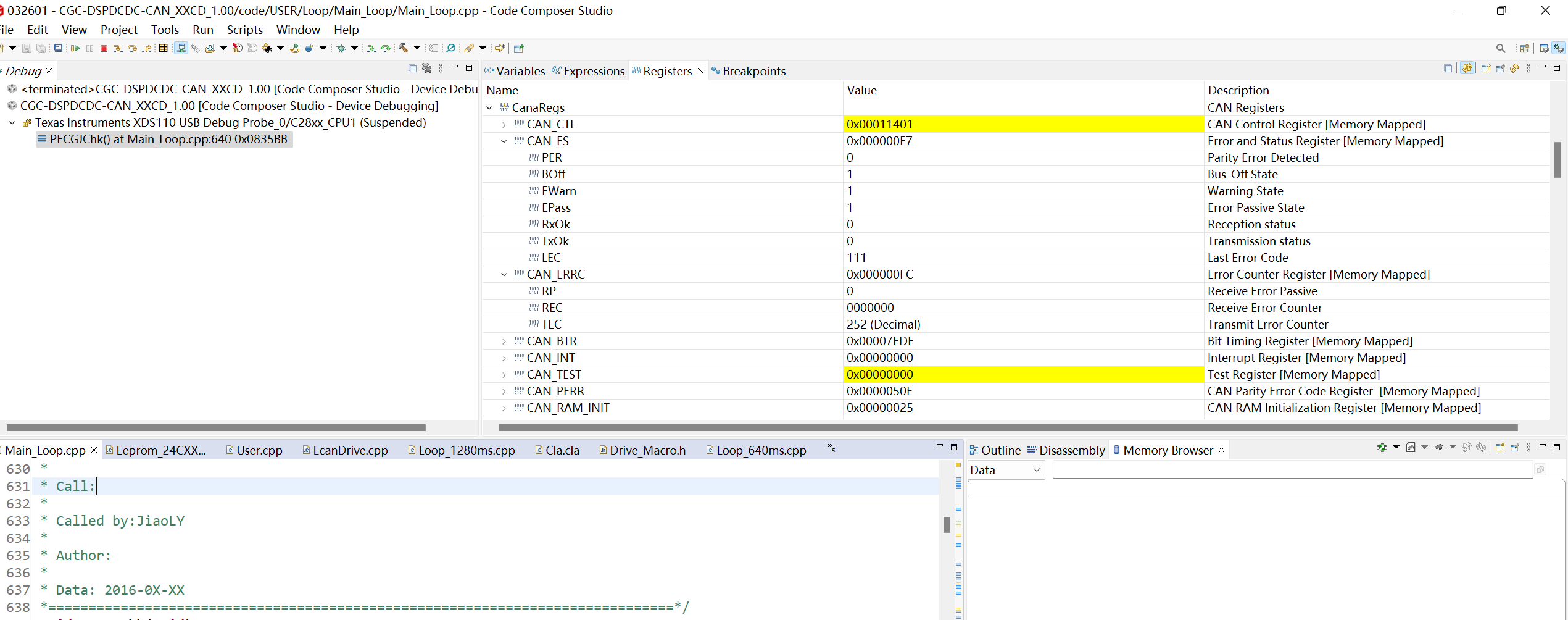
Thank you for sending the CAN frame. I do not see any anomalies on the waveform but i cannot see if ACK has been sent by the receiving node based on the picture. Can you zoom in near the CRC field and see if there is an ACK bit? Also once the first frame is sent by the transmitting node, can you immediately stop (break point) and display the CAN_ES register content?
Just to clarify, the use case that is failing is SYCLK = 100MHz and CAN Bit Timing is set to 125Kbps, correct?
I do not see any issues with the external clock configuration to produce the 100MHz SYSCLK for the chip.
Thanks and regards,
Joseph
I wasn't able to reply in time today because I had to deal with some other matters.
I wonder if you have conducted the replication test? We don't experience immediate malfunction right after power-on and start communication. Instead, the CAN bus will be shut down after a certain period of time.
Hi Wang,
Our validation tests connect several C28x including f28004x chips together through CAN bus with the tests running for several hours with no issue. What is the length of the CAN bus that you are using? Based from the previous CAN_ES log you have shared, it looks like there was a sudden increase in transmission error. Do you have the ability to connect to the debugger to inspect other registers like RESC (reset cause register) to see if reset may have toggled? Can you also check to see if SYSCLK is still configured at 100MHz? There is no suspected cause yet as to why CAN communication fails after sometime for your case so just looking for clues on what might have caused this to happen.
Regards,
Joseph
The length of the CAN bus about 1m.The CAN bus matching resistance is 60 Ω.Because using CAN_ES_TXOK to determine whether the transmission is complete in three machines.We use CAN_IF1CMD_BUSY judge in the function vEcanDrive_TxDataBufferProcess is no problem.So we no doubt RESET or SYSCLK. In use CAN_IF1CMD_BUSY if we one time in multiple frames use the function of vEcanDrive_Push2TxDataBuffer will be Lose frame. In out all test the Auto-Bus-On is disable. If the Auto-Bus-On is enable We can't see CAN bus shutdown. CAN bus is actually in the state of the switch switch switch.
Understood your point on RESER and SYSCLK issue. Auto-Bus On (ABO) enable is behaving correctly for your case. When enabled, CAN automatically recovers from the bus off condition due to transmission errors. Will enabling the ABO bit cause a problem in your application?
Need to understand in your setup where the bus error is coming from. Is there a CAN log you can look at to see the events happening in the bus before the bus off condition occurred?