This thread has been locked.

If you have a related question, please click the "Ask a related question" button in the top right corner. The newly created question will be automatically linked to this question.

TMS320F28377D: Why can't I use the serial port independently to program TMS320F28377D without the emulator?

Part Number: TMS320F28377D
Other Parts Discussed in Thread: C2000WARE

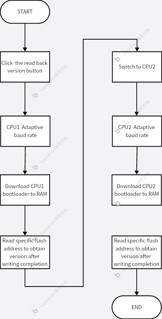
Our company has developed an upper computer for programming via serial port. There are two buttons for burning and reading back versions.Figures 1 and 2 show two workflows respectively. Each step of the process is controlled by instructions issued by the upper computer, and 28377 responds at the same time.

During the burning process, when whole chip erase of CPU2 flash, a response of 28377 could not be received, resulting in a burning failure. Upon inspection, it was found that no data was erased.

During the process of Read specific address to obtain version when reading a version, the last sector appears unreadable,Because after reading flash addresses 0x000BFFFA and 0x000BFFF8, 28377 did not respond.

When using a simulator to burn the boot program and send instructions to erase CPU1 and CPU2 on the entire chip, and then using the serial port to burn the program again, problems 1 and 2 were tested multiple times and no longer reproduced.The software and hardware used for testing are completely identical.So how can I independently use a serial burning program?
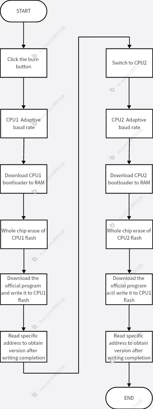
 

2a0653a4a4ac02dcffc7af7aa029c650.jpg

Figure 1


Figure 2.png

Figure 2


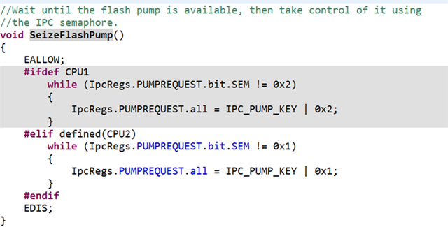
  • Would it be possible to share the bootloader code that runs on CPU2?  The only thing that comes to mind is that CPU2 has not grabbed/gained control of the flash pump semaphore, which would not allow it to erase the flash.

    Best,

    Matthew

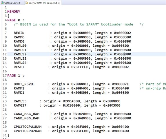
  • I'm sorry that I can't provide the source code program for CPU2, so I have provided screenshots of some of the functions, hoping this can help you find the problem.


    This is the CMD file for CPU2.


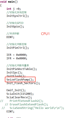
    This is the main function and initialization part function of CPU2


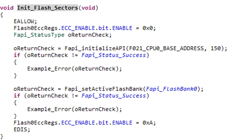
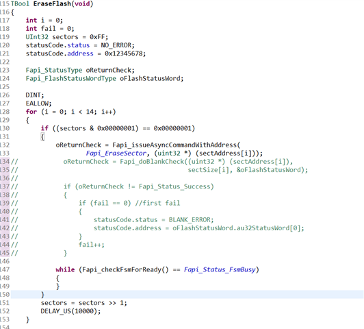
    This is the CPU2 erase flash function


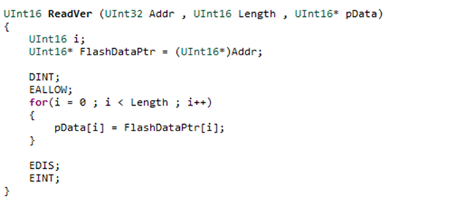
    This is the function for CPU2 to read flash data.


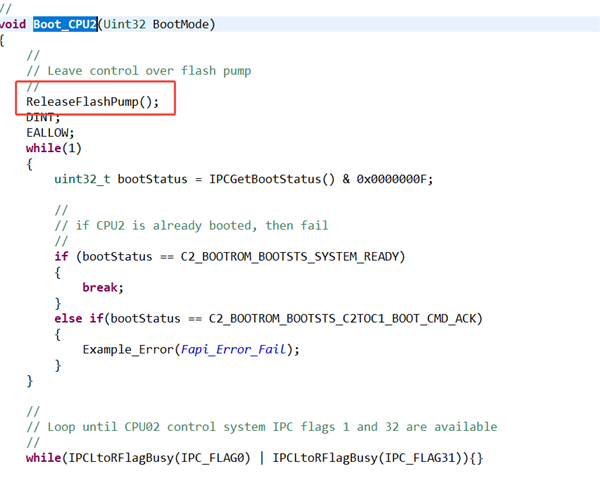
    In addition, I provided some functions of CPU1 to jump from CPU1 to CPU2.


  • I'm a bit behind in responding here, I'll take a look at what you provided and reply today.

    Best,

    Matthew

  • Okay, I will wait for your reply message.

  • Can you let me know which source file has the SeizeFlashPump Function?  I can't seem to find this function in our source files.  There should be a corresponding IPC receive command on the CPU1 to give control of the pump to CPU2.

    Best,

    Matthew

  • We called SeizeFlashPump function in main. c. Call the ReleaseFlashPump function in the boot_CPU2 function.

  • Cheng,

    Sorry for the lack of reply, I'm going to need some more time on this.  I will reply by the 17th.

    Best,
    Matthew

  • I will wait for your message Wishing you a wonderful weekend.

  • Cheng,

    Are you using our example flash kernels in C2000Ware located here: 

    C:\ti\c2000\C2000Ware_6_00_00_00\device_support\f2837xd\examples\dual\F2837xD_sci_flash_kernels\

    Based on your code I think this is what you are using, but want to make sure.

    I see this function in SCI_Boot.c, can you confirm which pins you have connected for the SCI comms?  I want to make sure we are passing the same pins for CPU2 to use in its boot

    void Assign_SCIA_IO_CPU2(Uint32 BootMode)
    {
        EALLOW;
        DevCfgRegs.CPUSEL5.bit.SCI_A = 1;    //SCIA connected to CPU2
        ClkCfgRegs.CLKSEM.all = 0xA5A50000;  //Allows CPU2 bootrom to take control
                                             //of clock configuration registers
        ClkCfgRegs.LOSPCP.all = 0x0007;
    
        if((BootMode & 0xF0) == 0x0)
        {
            //
            //OPTION 1
            //
            GPIO_SetupPinOptions(84, GPIO_OUTPUT, GPIO_ASYNC);
            GPIO_SetupPinMux(84,GPIO_MUX_CPU2,5);
            GPIO_SetupPinOptions(85, GPIO_INPUT, GPIO_ASYNC);
            GPIO_SetupPinMux(85,GPIO_MUX_CPU2,5);
        }
        else
        {
            //
            //OPTION 2
            //
            GPIO_SetupPinOptions(29, GPIO_OUTPUT, GPIO_ASYNC);
            GPIO_SetupPinMux(29,GPIO_MUX_CPU2,1);
            GPIO_SetupPinOptions(28, GPIO_INPUT, GPIO_ASYNC);
            GPIO_SetupPinMux(28,GPIO_MUX_CPU2,1);
        }
        EDIS;
    }

    To that end, have you made any modifications to that example code when you ported in for your use case?  

    Best,

    Matt

  • Yes, I called the function Assign _SCIA_IOU_CPU2 and made some modifications. The parameter BootMode I passed is 0.

  • Cheng,

    Since we are dealing with JTAG working/standalone not working; I'd like to focus on timing related issues in the code:

    This is from SCI_Boot.c in the CPU01 directory line 172.  My changes are encapsulated by //////

     while(IPCLtoRFlagBusy(IPC_FLAG0) | IPCLtoRFlagBusy(IPC_FLAG31)){}
    
        CpuSysRegs.PCLKCR7.bit.SCI_A = 1;
        DevCfgRegs.SOFTPRES7.bit.SCI_A = 1;
    /////////////////////////////////////////////////////////
        DELAY_US(1000);  // Replace the short for-loop
    //////////////////////////////////////////////////////
        CpuSysRegs.PCLKCR7.bit.SCI_A = 0;
        DevCfgRegs.SOFTPRES7.bit.SCI_A = 0;
    /////////////////////////////////////////////////////////
        DELAY_US(1000);  // Replace the short for-loop
    //////////////////////////////////////////////////////
    
        Assign_SCIA_IO_CPU2(BootMode);
        assignSharedRAMstoCPU2();
    /////////////////////////////////////////////////////////
        DELAY_US(10000);  // Replace the short for-loop
    //////////////////////////////////////////////////////   
        //
        // CPU1 to CPU2 IPC Boot Mode Register
        //
        IpcRegs.IPCBOOTMODE = C1C2_BROM_BOOTMODE_BOOT_FROM_SCI;
    
        //
        // CPU1 to CPU2 IPC Command Register
        //
        IpcRegs.IPCSENDCOM = C1C2_BROM_IPC_EXECUTE_BOOTMODE_CMD;

    In the F2837xD_sci_flash_kernels_cpu02.c file 

    Line 124

        
      ////////////////////////////////////////////////////////
      GPIO_WritePin(31, 1);  // Prove CPU2 is running, you can change the pin based on your PCB
      for(x = 0; x < 100000; x++){}
      GPIO_WritePin(31, 0);
    /////////////////////////////////////////////////////////  
        Uint16 x = 0;
        for(x = 0; x < 32676; x++){}
        for(x = 0; x < 32676; x++){}
    
        IpcRegs.IPCBOOTSTS = C2_BOOTROM_BOOTSTS_SYSTEM_READY;
        while(IpcRegs.IPCBOOTMODE != C1C2_BROM_BOOTMODE_BOOT_FROM_SCI){}
    
        EINT; //enable global interrupt INTM
        ERTM; //enable global realtime interrupt

    And then at line 140, let's re-init the SCI to make sure this didn't get corrupted

    SeizeFlashPump();
        Init_Flash_Sectors();
        //put GetFunction here
    ///////////////////////////////////////////    
        SCIA_Init(SCI_BOOT);  // ADD THIS LINE
    //////////////////////////////////////////    
        uint32_t EntryAddr = SCI_GetFunction();
    
    //
    // Leave control over flash pump
    //
        SignalCPU1();
        return EntryAddr; //load entry address of application into
                          //RPC: return program counter
    }

    Best,
    Matthew

    You will also need to add these prototypes:

    extern void SCIA_Init(Uint32 BootMode);
    extern void GPIO_WritePin(Uint32 pin, Uint32 outVal); to the cpu02.c file

    Let's see if extending some of these timings gets things to work in standalone mode.

  • I have successfully found a solution, which is to block the code in the following image. When I keep this part of the program, it will crash here. After blocking this part of the code, the internal flash erase, read and write functions can be used normally through SCI. I think you can tell me the reason for this problem, thank you for that.

  • Cheng,

    Thank you for this information, this does explain the issue.  

    The Fapi_issueAsyncCommandWithAddress, will not wait until the operation (in this case flash erase) is complete before returning.  Since the blank check is called immediately after this, the erase is not guaranteed to be complete.  So the blank check either stalls or fails in this case.

    The correct implementation with any Async command, is to check the FSM to make sure it is not busy before executing another API call as shown in the code below.

    If you insert the while (Fapi_checkFsmForReady()...to your code after the Async command this should also fix things.

    Best,

    Matthew

    oReturnCheck = Fapi_issueAsyncCommandWithAddress(Fapi_EraseSector,
                       (uint32 *)Bzero_SectorC_start);
    
        //
        // Wait until FSM is done with erase sector operation.
        //
        while (Fapi_checkFsmForReady() != Fapi_Status_FsmReady)
        {
        }
    
        //
        // Verify that Sector C is erased. The erase step itself does verification
        // as it goes. This verify is a second verification that can be done.
        //
        oReturnCheck = Fapi_doBlankCheck((uint32 *)Bzero_SectorC_start,
                       Bzero_16KSector_u32length,
                       &oFlashStatusWord);