Part Number: TMS320F28379D
Other Parts Discussed in Thread: SYSCONFIG, UNIFLASH
Hello, everyone
We are developing a communication device using TMS320F28379D with the following configuration on both CPU1 and CPU2:
-
Secondary Bootloader (SBL)
-
Application (APP)
-
DCSM enabled
Environment:
Device: TMS320F28379D
Boot Mode:
-
- SCI Boot (firmware update using sci_flash_kernel)
- Flash Boot (SBL + APP)
CCS Version: 12.7.1
Flash Memory Map:
# CPU1
-
- origin = 0x080000, length = 0x000002 → SBL BEGIN (codestart) ... FLASHA
- origin = 0x082000, length = 0x001FF0 → SBL program ... FLASHB
- origin = 0x084000, length = 0x000002 → APP BEGIN (codestart) ... FLASHC
- origin = 0x086000, length = 0x022000 → APP program ... FLASHD/E/F/G/H
# CPU2
-
- origin = 0x080000, length = 0x000002 → SBL BEGIN (codestart) ... FLASHA
- origin = 0x082000, length = 0x002000 → SBL program ... FLASHB
- origin = 0x084000, length = 0x000002 → APP BEGIN (codestart) ... FLASHC
- origin = 0x084002, length = 0x023FFE → APP program ... FLASHC/E/F/G/H
Expected Behavior:
With the SBL + APP configuration, the system boots and operates as expected.
When only CPU2 has DCSM enabled, it run as expected.
Issue:
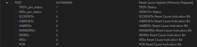
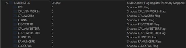
When DCSM is enabled (SBL + APP + DCSM), the system does not start.
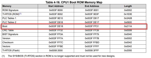
When debugging the CPU1 SBL with the CCS debugger, execution stops at:
_system_post_cinit() [stop address] (an error occurred: failed to parse the previous frame FP")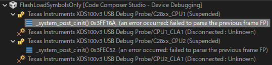
Execution does not reach the main() function of the CPU1 SBL.
Notes:
We suspect that there is an issue in the DCSM configuration, but we have not been able to determine which setting may be causing the problem.
Due to IP restrictions, we can only share excerpts.
We will upload the following files related to CPU1 SBL/APP:
-
- main()
- dcsm.asm
- Linker Command file
Could anyone point out possible issues in our DCSM configuration or memory map that could cause this behavior?
Any help in identifying the cause of this issue would be greatly appreciated.
CPU1
SBL
main()
#include "key.h"

#define BRANCH_APP  "    LB 0x084000"

void main()
{

    GenerateKey();

    asm(BRANCH_APP);
}
dcsm.asm
;----------------------------------------------------------------------
; Zone 1
;----------------------------------------------------------------------
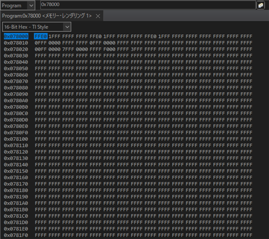
     .sect "dcsm_otp_z1_linkpointer"
      .retain
      .long 0x1FFFFFFC
      .long 0xFFFFFFFF     ;Reserved
      .long 0x1FFFFFFC
      .long 0xFFFFFFFF     ;Reserved
      .long 0x1FFFFFFC
      .long 0xFFFFFFFF     ;Reserved

     .sect "dcsm_otp_z1_pswdlock"
      .retain
      .long 0xFFFFFFF0
      .long 0xFFFFFFFF     ;Reserved

     .sect "dcsm_otp_z1_crclock"
      .retain
      .long 0xFFFFFFFF
      .long 0xFFFFFFFF     ;Reserved

     .sect "dcsm_otp_z1_jtaglock"
      .retain
      .long 0xFFFFFFFF
      .long 0xFFFFFFFF     ;Reserved
;;     .sect "dcsm_otp_z1_bootctrl"
;;      .retain
;;      .long 0xFFFFFFFF     ;Reserved
;;      .long 0x49550B5A

     .sect "dcsm_zsel_z1"
      .retain
      .long 0x000000FF       ;Z1-EXEONLYRAM
      .long 0x00003FFF      ;Z1-EXEONLYSECT
      .long 0x3000F555          ;Z1-GRABRAM  - LS0-5 RAM Secured
      .long 0x0FFF5555         ;Z1-GRABSECT - FLASHA-H Secured

      .long 0xFFFFFFFF  ; Confidentiality
      .long 0xFFFFFFFF
      .long 0xFFFFFFFF
      .long 0xFFFFFFFF


;----------------------------------------------------------------------

; For code security operation,after development has completed, prior to
; production, all other zone select block locations should be programmed
; to 0x0000 for maximum security.
; If the first zone select block at offset 0x10 is used, the section
; "dcsm_rsvd_z1" can be used to program these locations to 0x0000.
; This code is commented out for development.

;       .sect "dcsm_rsvd_z1"
;        .loop (1e0h)
;              .int 0x0000
;        .endloop


;----------------------------------------------------------------------
; Zone 2
;----------------------------------------------------------------------
;;     .sect "dcsm_otp_z2_linkpointer"
;;      .retain
;;      .long 0x1FFFFFFF
;;      .long 0xFFFFFFFF     ;Reserved
;;      .long 0x1FFFFFFF
;;      .long 0xFFFFFFFF     ;Reserved
;;      .long 0x1FFFFFFF
;;      .long 0xFFFFFFFF     ;Reserved
;;
;;     .sect "dcsm_otp_z2_pswdlock"
;;      .retain
;;      .long 0xFFFFFFFF
;;      .long 0xFFFFFFFF     ;Reserved
;;
;;     .sect "dcsm_otp_z2_crclock"
;;      .retain
;;      .long 0xFFFFFFFF
;;      .long 0xFFFFFFFF     ;Reserved
;;     .sect "dcsm_otp_z2_jtaglock"
;;      .retain
;;      .long 0xFFFFFFFF
;;      .long 0xFFFFFFFF     ;Reserved
;;
;;     .sect "dcsm_otp_z2_bootctrl"
;;      .retain
;;      .long 0xFFFFFFFF     ;Reserved
;;      .long 0x49550B5A
;;
;;     .sect "dcsm_zsel_z2"
;;      .retain
;;      .long 0x000000FF       ;z2-EXEONLYRAM
;;      .long 0x00003FFF      ;z2-EXEONLYSECT
;;      .long 0x3000FFFF          ;z2-GRABRAM
;;      .long 0x0FFFFFFF         ;z2-GRABSECT
;;
;;      .long 0xFFFFFFFF
;;      .long 0xFFFFFFFF
;;      .long 0xFFFFFFFF
;;      .long 0xFFFFFFFF


;----------------------------------------------------------------------

; For code security operation,after development has completed, prior to
; production, all other zone select block locations should be programmed
; to 0x0000 for maximum security.
; If the first zone select block at offset 0x10 is used, the section
; "dcsm_rsvd_z2" can be used to program these locations to 0x0000.
; This code is commented out for development.

;       .sect "dcsm_rsvd_z2"
;        .loop (1e0h)
;              .int 0x0000
;        .endloop


;----------------------------------------------------------------------
; End of file
;----------------------------------------------------------------------
Linker Command file
MEMORY
{
PAGE 0 :  /* Program Memory */
          /* Memory (RAM/FLASH) blocks can be moved to PAGE1 for data allocation */
          /* BEGIN is used for the "boot to Flash" bootloader mode   */

    BEGIN            : origin = 0x080000, length = 0x000008
    RAMM0            : origin = 0x000122, length = 0x0002DE
//	RAMD0            : origin = 0x00B000, length = 0x000800	// mov: PAGE 0 -> 1
    RAMLS0_5         : origin = 0x008000, length = 0x003000
    RAMGS10          : origin = 0x016000, length = 0x001000
    RESET            : origin = 0x3FFFC0, length = 0x000002

    /* Flash sectors */
    FLASHA           : origin = 0x080008, length = 0x001FF8	/* on-chip Flash */
    FLASHB_SBL       : origin = 0x082000, length = 0x001FF0	/* on-chip Flash (my secondary bootloader area) */
    FLASHB_FUNCENTRY : origin = 0x083FF0, length = 0x000010	/* on-chip Flash (CheckKey-related logic entory-point area for apps in the secondary bootloader) */
//  FLASHC           : origin = 0x084000, length = 0x002000	/* on-chip Flash (my app area) */
//  FLASHD           : origin = 0x086000, length = 0x002000	/* on-chip Flash (my app area) */
//  FLASHE           : origin = 0x088000, length = 0x008000	/* on-chip Flash (my app area) */
//  FLASHF           : origin = 0x090000, length = 0x008000	/* on-chip Flash (my app area) */
//  FLASHG           : origin = 0x098000, length = 0x008000	/* on-chip Flash (my app area) */
//  FLASHH           : origin = 0x0A0000, length = 0x008000	/* on-chip Flash (my app area) */
//  FLASHI           : origin = 0x0A8000, length = 0x008000	/* on-chip Flash */
//  FLASHJ           : origin = 0x0B0000, length = 0x008000	/* on-chip Flash */
//  FLASHK           : origin = 0x0B8000, length = 0x002000	/* on-chip Flash */
//  FLASHL           : origin = 0x0BA000, length = 0x002000	/* on-chip Flash */
//  FLASHM           : origin = 0x0BC000, length = 0x002000	/* on-chip Flash */
//  FLASHN           : origin = 0x0BE000, length = 0x001FF0	/* on-chip Flash */

//   FLASHN_RSVD     : origin = 0x0BFFF0, length = 0x000010    /* Reserve and do not use for code as per the errata advisory "Memory: Prefetching Beyond Valid Memory" */

#ifdef _USE_BOOT_LOADER
//------------------------------------------------------------------------------
// DCSM Configuration
//------------------------------------------------------------------------------
   /* Z1 OTP.  LinkPointers */
   DCSM_OTP_Z1_LINKPOINTER   : origin = 0x78000, length = 0x00000C
   /* Z1 OTP.  GPREG1/GPREG2 */
   DCSM_OTP_Z1_GPREG         : origin = 0x7800C, length = 0x000004
   /* Z1 OTP.  PSWDLOCK/RESERVED */
   DCSM_OTP_Z1_PSWDLOCK	    : origin = 0x78010, length = 0x000004
   /* Z1 OTP.  CRCLOCK/RESERVED */
   DCSM_OTP_Z1_CRCLOCK	    : origin = 0x78014, length = 0x000004
   /* Z1 OTP.  RESERVED/JTAGLOCK - F28379D JATGLOCK Not supported */
   DCSM_OTP_Z1_JTAGLOCK	    : origin = 0x78018, length = 0x000004
   /* Z1 OTP.  RESERVED/BOOTCTRL */
   DCSM_OTP_Z1_BOOTCTRL	    : origin = 0x7801C, length = 0x000004

   /* DCSM Z1 Zone Select Contents (!!Movable!!) */
   /* Z1 OTP.  Z1 password locations / Flash and RAM partitioning */
   DCSM_ZSEL_Z1_P0	        : origin = 0x78020, length = 0x000010

   /* Z2 OTP.  LinkPointers */
   DCSM_OTP_Z2_LINKPOINTER	: origin = 0x78200, length = 0x00000C
   /* Z2 OTP.  GPREG1/GPREG2 */
   DCSM_OTP_Z2_GPREG	        : origin = 0x7820C, length = 0x000004
   /* Z2 OTP.  PSWDLOCK/RESERVED */
   DCSM_OTP_Z2_PSWDLOCK	    : origin = 0x78210, length = 0x000004
   /* Z2 OTP.  CRCLOCK/RESERVED */
   DCSM_OTP_Z2_CRCLOCK	    : origin = 0x78214, length = 0x000004
   /* Z2 OTP.  RESERVED/JTAGLOCK - F28379D JATGLOCK Not supported */
   DCSM_OTP_Z2_JTAGLOCK	    : origin = 0x78218, length = 0x000004
   /* Z2 OTP.  GPREG3/BOOTCTRL */
   DCSM_OTP_Z2_BOOTCTRL	    : origin = 0x7821C, length = 0x000004

   /* DCSM Z2 Zone Select Contents (!!Movable!!) */
   /* Z2 OTP.  Z2 password locations / Flash and RAM partitioning  */
   DCSM_ZSEL_Z2_P0	        : origin = 0x78220, length = 0x000010
#endif	/* _USE_BOOT_LOADER */

PAGE 1 : /* Data Memory */
         /* Memory (RAM/FLASH) blocks can be moved to PAGE0 for program allocation */

    BOOT_RSVD        : origin = 0x000002, length = 0x000121     /* Part of M0, BOOT rom will use this for stack */
    RAMM1            : origin = 0x000400, length = 0x0003F8     /* on-chip RAM block M1 */
//  RAMM1_RSVD       : origin = 0x0007F8, length = 0x000008     /* Reserve and do not use for code as per the errata advisory "Memory: Prefetching Beyond Valid Memory" */
//	RAMD1            : origin = 0x00B800, length = 0x000800     //trm stack area : TRM_STACK_WSIZE:512 * 4
	RAMD0_1          : origin = 0x00B000, length = 0x001000	    //trm stack area : TRM_STACK_WSIZE:512 * 8

    CLA1_MSGRAMLOW   : origin = 0x001480, length = 0x000080     /* CLA to CPU Message RAM, DCSM secure */
    CLA1_MSGRAMHIGH  : origin = 0x001500, length = 0x000080     /* CPU to CLA Message RAM, DCSM secure */

    //**************************************************************************
    // @CAUTION
    //   The GSx_RAM (Global Shared RAM) should be assigned to either CPU by the GSxMSEL register.
    //**************************************************************************
 /*
    RAMGS0      : origin = 0x00C000, length = 0x001000
    RAMGS1      : origin = 0x00D000, length = 0x001000
    RAMGS2      : origin = 0x00E000, length = 0x001000
    RAMGS3      : origin = 0x00F000, length = 0x001000
    RAMGS4      : origin = 0x010000, length = 0x001000
    RAMGS5      : origin = 0x011000, length = 0x001000
    RAMGS6      : origin = 0x012000, length = 0x001000
    RAMGS7      : origin = 0x013000, length = 0x001000
    RAMGS8      : origin = 0x014000, length = 0x001000
    RAMGS9      : origin = 0x015000, length = 0x001000
    ^----CPU2   CPU1----v
    RAMGS10     : origin = 0x016000, length = 0x001000

//  RAMGS11     : origin = 0x017000, length = 0x000FF8      // Uncomment for F28374D, F28376D devices //
//  RAMGS11_RSVD : origin = 0x017FF8, length = 0x000008     // Reserve and do not use for code as per the errata advisory "Memory: Prefetching Beyond Valid Memory" //

    RAMGS11     : origin = 0x017000, length = 0x001000      // Only Available on F28379D, F28378D, F28377D, F28375D devices. Remove line on other devices. //
    RAMGS12     : origin = 0x018000, length = 0x001000      // Only Available on F28379D, F28378D, F28377D, F28375D devices. Remove line on other devices. //
    RAMGS13     : origin = 0x019000, length = 0x001000      // Only Available on F28379D, F28378D, F28377D, F28375D devices. Remove line on other devices. //
    RAMGS14     : origin = 0x01A000, length = 0x001000      // Only Available on F28379D, F28378D, F28377D, F28375D devices. Remove line on other devices. //
    RAMGS15     : origin = 0x01B000, length = 0x001000      // Only Available on F28379D, F28378D, F28377D, F28375D devices. Remove line on other devices. //
*/
// --- RAMGS10 - RAMGS15 are used for CPU1 ---
//    RAMGS11_15		  : origin = 0x017000, length = 0x005000
    RAMGS11_15	    : origin = 0x017000, length = 0x004FE0
    RAMGS15_KEY     : origin = 0x01BFE0, length = 0x000010

    CPU2TOCPU1RAM   : origin = 0x03F800, length = 0x000400
    CPU1TOCPU2RAM   : origin = 0x03FC00, length = 0x000400
}

SECTIONS
{
   /* Allocate program areas: */
   .cinit              : > FLASHB_SBL      PAGE = 0, ALIGN(8)
   .pinit              : > FLASHB_SBL      PAGE = 0, ALIGN(8)
   .text               : > FLASHB_SBL      PAGE = 0, ALIGN(8)
   codestart           : > BEGIN       PAGE = 0, ALIGN(8)

   /* Allocate uninitalized data sections: */
   .stack              : > RAMM1       PAGE = 1
   .ebss               : > RAMGS11_15  PAGE = 1
   .esysmem            : > RAMGS11_15  PAGE = 1
   .key                : > RAMGS15_KEY  PAGE = 1, type=NOINIT
// .econst             : >> FLASHF      PAGE = 0, ALIGN(8)
   .econst             : > FLASHB_SBL      PAGE = 0, ALIGN(8)
   .switch             : > FLASHB_SBL      PAGE = 0, ALIGN(8)

   .funcentry          : > FLASHB_FUNCENTRY PAGE = 0, ALIGN(8)

   .product_info :
   {
       *(.product_info)
   } > FLASHB_SBL PAGE = 0, ALIGN(8)

   .reset              : > RESET,      PAGE = 0, TYPE = DSECT /* not used, */

#ifdef __TI_COMPILER_VERSION__
    #if __TI_COMPILER_VERSION__ >= 15009000
        #if defined(__TI_EABI__)
        	GROUP
        	{
                .TI.ramfunc
                { -l F021_API_F2837xD_FPU32.lib }
            } LOAD = FLASHB_SBL,
              RUN = RAMLS0_5,
              LOAD_START(RamfuncsLoadStart),
              LOAD_SIZE(RamfuncsLoadSize),
              LOAD_END(RamfuncsLoadEnd),
              RUN_START(RamfuncsRunStart),
              RUN_SIZE(RamfuncsRunSize),
              RUN_END(RamfuncsRunEnd),
              PAGE = 0, ALIGN(8)
        #else
        	GROUP
        	{
                .TI.ramfunc
                { -l F021_API_F2837xD_FPU32.lib }
            } LOAD = FLASHB_SBL,
              RUN = RAMLS0_5,
              LOAD_START(_RamfuncsLoadStart),
              LOAD_SIZE(_RamfuncsLoadSize),
              LOAD_END(_RamfuncsLoadEnd),
              RUN_START(_RamfuncsRunStart),
              RUN_SIZE(_RamfuncsRunSize),
              RUN_END(_RamfuncsRunEnd),
              PAGE = 0, ALIGN(8)
        #endif
    #else
        GROUP
        {
            ramfuncs
            { -l F021_API_F2837xD_FPU32.lib }
        } LOAD = FLASHB_SBL,
          RUN = RAMLS0_5,
          LOAD_START(_RamfuncsLoadStart),
          LOAD_SIZE(_RamfuncsLoadSize),
          LOAD_END(_RamfuncsLoadEnd),
          RUN_START(_RamfuncsRunStart),
          RUN_SIZE(_RamfuncsRunSize),
          RUN_END(_RamfuncsRunEnd),
          PAGE = 0, ALIGN(8)
    #endif

#endif

   /* The following section definitions are required when using the IPC API Drivers */
    GROUP : > CPU1TOCPU2RAM, PAGE = 1
    {
        PUTBUFFER
        PUTWRITEIDX
        GETREADIDX
    }

    GROUP : > CPU2TOCPU1RAM, PAGE = 1
    {
        GETBUFFER :    TYPE = DSECT
        GETWRITEIDX :  TYPE = DSECT
        PUTREADIDX :   TYPE = DSECT
    }

    Cla1ToCpuMsgRAM  : > CLA1_MSGRAMLOW,   PAGE = 1    /* Link to CLA Message RAM */
    CpuToCla1MsgRAM  : > CLA1_MSGRAMHIGH,  PAGE = 1    /* Link to CLA Message RAM */

#ifdef _USE_BOOT_LOADER
//------------------------------------------------------------------------------
// DCSM Configuration
//------------------------------------------------------------------------------
   dcsm_otp_z1_linkpointer 	: > DCSM_OTP_Z1_LINKPOINTER		PAGE = 0
   dcsm_otp_z1_pswdlock		: > DCSM_OTP_Z1_PSWDLOCK		PAGE = 0
   dcsm_otp_z1_crclock		: > DCSM_OTP_Z1_CRCLOCK			PAGE = 0
   /* F28379D JATGLOCK Not supported */
    dcsm_otp_z1_jtaglock    : > DCSM_OTP_Z1_JTAGLOCK        PAGE = 0, type = DSECT
   dcsm_otp_z1_bootctrl		: > DCSM_OTP_Z1_BOOTCTRL		PAGE = 0, type = DSECT
   dcsm_zsel_z1				: > DCSM_ZSEL_Z1_P0				PAGE = 0

   dcsm_otp_z2_linkpointer	: > DCSM_OTP_Z2_LINKPOINTER		PAGE = 0, type = DSECT
   dcsm_otp_z2_pswdlock		: > DCSM_OTP_Z2_PSWDLOCK		PAGE = 0, type = DSECT
   dcsm_otp_z2_crclock		: > DCSM_OTP_Z2_CRCLOCK			PAGE = 0, type = DSECT
   /* F28379D JATGLOCK Not supported */
    dcsm_otp_z2_jtaglock    : > DCSM_OTP_Z2_JTAGLOCK        PAGE = 0, type = DSECT
   dcsm_otp_z2_bootctrl		: > DCSM_OTP_Z2_BOOTCTRL		PAGE = 0, type = DSECT
   dcsm_zsel_z2				: > DCSM_ZSEL_Z2_P0				PAGE = 0, type = DSECT
#endif	/* _USE_BOOT_LOADER */
}

/*
//===========================================================================
// End of file.
//===========================================================================
*/
APP
main()
void main(void)
{
#ifdef _USE_BOOT_LOADER
    // Secondary Bootloader(FLASHB) function: call "CheckKey".
    // @NOTE:
    //   If the key check fails, the "CheckKey" function will enter
    //   an infinite loop (while(FOREVER)).
    SBL_FUNCS[0]();
#endif
    Hardware_Init();
...

#ifdef _FLASH
    //--- Send boot command to allow the CPU2 application to begin execution ---
    //#warning    no IPCBootCPU2
    IPCBootCPU2(C1C2_BROM_BOOTMODE_BOOT_FROM_FLASH);
#endif
...
}
Linker Command file
// @NOTE:
//   This definition was added as _USE_BOOT_LOADER in
//     Build > C2000 Linker > Advanced Options: "Predefined preprocessor macro _name_ to _value_ (--define)"
//   of the build configuration: CPU1_USE_BOOTLOADER.
//#define _USE_BOOT_LOADER

MEMORY
{
PAGE 0:    /* Program Memory */
          /* Memory (RAM/FLASH) blocks can be moved to PAGE1 for data allocation */
          /* BEGIN is used for the "boot to Flash" bootloader mode   */
#ifdef _USE_BOOT_LOADER
	BEGIN           	: origin = 0x084000, length = 0x000002 //FLASH C
#else
	BEGIN           	: origin = 0x080000, length = 0x000002
#endif
	RAMM0            : origin = 0x000122, length = 0x0002DE
//	RAMD0            : origin = 0x00B000, length = 0x000800	// mov: PAGE 0 -> 1
	RAMLS0_5         : origin = 0x008000, length = 0x003000
 	RAMGS10          : origin = 0x016000, length = 0x001000
	RESET            : origin = 0x3FFFC0, length = 0x000002

	/* Flash sectors */
#ifdef _USE_BOOT_LOADER
//  FLASHA           : origin = 0x080002, length = 0x001FFE	/* on-chip Flash */
//  FLASHB           : origin = 0x082000, length = 0x002000	/* on-chip Flash (my boot loader area) */
    FLASHC           : origin = 0x084002, length = 0x001FFE	/* on-chip Flash */
#else
    FLASHA           : origin = 0x080002, length = 0x001FFE	/* on-chip Flash */
//  FLASHB           : origin = 0x082000, length = 0x002000	/* on-chip Flash (my boot loader area) */
    FLASHC           : origin = 0x084000, length = 0x002000	/* on-chip Flash */
#endif
    FLASHD           : origin = 0x086000, length = 0x002000	/* on-chip Flash */
    FLASHE           : origin = 0x088000, length = 0x008000	/* on-chip Flash */
    FLASHF           : origin = 0x090000, length = 0x008000	/* on-chip Flash */
    FLASHG           : origin = 0x098000, length = 0x008000	/* on-chip Flash */
    FLASHH           : origin = 0x0A0000, length = 0x008000	/* on-chip Flash */
//  FLASHI           : origin = 0x0A8000, length = 0x008000	/* on-chip Flash */
//  FLASHJ           : origin = 0x0B0000, length = 0x008000	/* on-chip Flash */
//  FLASHK           : origin = 0x0B8000, length = 0x002000	/* on-chip Flash */
//  FLASHL           : origin = 0x0BA000, length = 0x002000	/* on-chip Flash */
//  FLASHM           : origin = 0x0BC000, length = 0x002000	/* on-chip Flash */
//  FLASHN           : origin = 0x0BE000, length = 0x002000	/* on-chip Flash */

PAGE 1 :   /* Data Memory */
         /* Memory (RAM/FLASH) blocks can be moved to PAGE0 for program allocation */

    BOOT_RSVD       : origin = 0x000002, length = 0x000120     /* Part of M0, BOOT rom will use this for stack */
	RAMM1           : origin = 0x000400, length = 0x000400     /* on-chip RAM block M1 */
//	RAMD1           : origin = 0x00B800, length = 0x000800	   //trm stack area : TRM_STACK_WSIZE:512 * 4
	RAMD0_1         : origin = 0x00B000, length = 0x001000	   //trm stack area : TRM_STACK_WSIZE:512 * 8

    CLA1_MSGRAMLOW   : origin = 0x001480, length = 0x000080  /* CLA to CPU Message RAM, DCSM secure */
    CLA1_MSGRAMHIGH  : origin = 0x001500, length = 0x000080  /* CPU to CLA Message RAM, DCSM secure */

/*
   RAMGS0           : origin = 0x00C000, length = 0x001000
   :
   RAMGS9           : origin = 0x015000, length = 0x001000
   ^----CPU2   CPU1----v
   RAMGS10          : origin = 0x016000, length = 0x001000
   :
   RAMGS15          : origin = 0x01B000, length = 0x001000
*/

// --- RAMGS10 - RAMGS15 are used for CPU1 ---
//	RAMGS11_15		: origin = 0x017000, length = 0x005000
   RAMGS11_15	   : origin = 0x017000, length = 0x004FE0
   RAMGS15_KEY     : origin = 0x01BFE0, length = 0x000010	/* check key values - Collaboration with Bootloader */

   CPU2TOCPU1RAM   : origin = 0x03F800, length = 0x000400
   CPU1TOCPU2RAM   : origin = 0x03FC00, length = 0x000400
}


SECTIONS
{

   /* Allocate program areas: */
   .cinit              : > FLASHD, ALIGN(8)		PAGE = 0
   .pinit              : > FLASHD, ALIGN(8)		PAGE = 0
   .text               : >> FLASHD | FLASHE, ALIGN(8)	PAGE = 0
   codestart           : > BEGIN,  ALIGN(8)		PAGE = 0

#ifdef __TI_COMPILER_VERSION__
    #if __TI_COMPILER_VERSION__ >= 15009000
        GROUP
        {
            .TI.ramfunc
            //{ -l F021_API_F2837xD_FPU32.lib}

        } LOAD = FLASHD,
          RUN  = RAMLS0_5,
          LOAD_START(_RamfuncsLoadStart),
          LOAD_SIZE(_RamfuncsLoadSize),
          LOAD_END(_RamfuncsLoadEnd),
          RUN_START(_RamfuncsRunStart),
          RUN_SIZE(_RamfuncsRunSize),
          RUN_END(_RamfuncsRunEnd),
          PAGE = 0, ALIGN(8)
    #else
        GROUP
        {
            ramfuncs
            { -l F021_API_F2837xD_FPU32.lib}

        } LOAD = FLASHD,
          RUN  = RAMLS0_5,
          LOAD_START(_RamfuncsLoadStart),
          LOAD_SIZE(_RamfuncsLoadSize),
          LOAD_END(_RamfuncsLoadEnd),
          RUN_START(_RamfuncsRunStart),
          RUN_SIZE(_RamfuncsRunSize),
          RUN_END(_RamfuncsRunEnd),
          PAGE = 0, ALIGN(8)
    #endif
#endif

   //testOutput		: > RAMGS14, PAGE = 1

   /* Allocate uninitalized data sections: */
   .stack              : > RAMM1       PAGE = 1
//   .trmstack           : > RAMD1	    PAGE = 1 //@ trm stack area
   .trmstack           : > RAMD0_1	   PAGE = 1 //@ trm stack area
   .ebss               : > RAMGS11_15  PAGE = 1
   .esysmem            : > RAMGS11_15  PAGE = 1

   .comm_data          : > RAMGS11_15   PAGE = 1,HIGH //@

   .key                : > RAMGS15_KEY  PAGE = 1, type=NOINIT	/* check key values - Collaboration with Bootloader */

   /* Initalized sections go in Flash */
   .econst             : >> FLASHF | FLASHG, ALIGN(8)	PAGE = 0
   .switch             : > FLASHD, ALIGN(8)				PAGE = 0

   .reset              : > RESET,     PAGE = 0, TYPE = DSECT /* not used, */

   /* Flash Programming Buffer - Unused... */
//   FapiBuffDataSection : > RAMD1, PAGE = 1, ALIGN(4)
//   FapiBuffDataSection : > RAMD0_1, PAGE = 1, ALIGN(4)

   /* The following section definitions are required when using the IPC API Drivers */
    GROUP : > CPU1TOCPU2RAM, PAGE = 1
    {
        PUTBUFFER
        PUTWRITEIDX
        GETREADIDX
    }

    GROUP : > CPU2TOCPU1RAM, PAGE = 1
    {
        GETBUFFER :    TYPE = DSECT
        GETWRITEIDX :  TYPE = DSECT
        PUTREADIDX :   TYPE = DSECT
    }

    /* CLA specific sections (CLA unused on CPU1) */
//    .scratchpad      : > RAMLS1_2,  PAGE = 1   /* Scratchpad memory for the CLA C Compiler */
//    {
//        . += 0x100;
//    }
//    Cla1Data1        : > RAMLS1_2 ,  PAGE = 1    /* Link to CLA Data RAM */
//
//    Cla1Prog         :  LOAD = FLASHH
//                        RUN = RAMLS5
//                        LOAD_START(_Cla1funcsLoadStart),
//                        LOAD_END(_Cla1funcsLoadEnd),
//                        RUN_START(_Cla1funcsRunStart),
//                        LOAD_SIZE(_Cla1funcsLoadSize),
//                        PAGE = 0, ALIGN(8)
//
    Cla1ToCpuMsgRAM  : > CLA1_MSGRAMLOW,   PAGE = 1    /* Link to CLA Message RAM */
    CpuToCla1MsgRAM  : > CLA1_MSGRAMHIGH,  PAGE = 1    /* Link to CLA Message RAM */

}

/*
//===========================================================================
// End of file.
//===========================================================================
*/
CPU2
SBL
main()
#define BRANCH_APP  "    LB 0x084000"

void main()
{
    asm(BRANCH_APP);
}
dcsm.asm
;----------------------------------------------------------------------
; Zone 1
;----------------------------------------------------------------------
     .sect "dcsm_otp_z1_linkpointer"
      .retain
      .long 0x1FFFFFFF
      .long 0xFFFFFFFF     ;Reserved
      .long 0x1FFFFFFF
      .long 0xFFFFFFFF     ;Reserved
      .long 0x1FFFFFFF
      .long 0xFFFFFFFF     ;Reserved

     .sect "dcsm_otp_z1_pswdlock"
      .retain
      .long 0xFFFFFFF0
      .long 0xFFFFFFFF     ;Reserved

     .sect "dcsm_otp_z1_crclock"
      .retain
      .long 0xFFFFFFFF
      .long 0xFFFFFFFF     ;Reserved

     .sect "dcsm_otp_z1_jtaglock"
      .retain
      .long 0xFFFFFFFF
      .long 0xFFFFFFFF     ;Reserved
;;     .sect "dcsm_otp_z1_bootctrl"
;;      .retain
;;      .long 0xFFFFFFFF     ;Reserved
;;      .long 0x49550B5A

     .sect "dcsm_zsel_z1"
      .retain
      .long 0x000000FF       ;Z1-EXEONLYRAM
      .long 0x00003FFF      ;Z1-EXEONLYSECT
      .long 0x1000F55D          ;Z1-GRABRAM - CLA, LS0/LS2-5 RAM Secured
      .long 0x0FFF5555         ;Z1-GRABSECT - FLASHA-H Secured

      .long 0xFFFFFFFF  ; Confidentiality
      .long 0xFFFFFFFF
      .long 0xFFFFFFFF
      .long 0xFFFFFFFF


;----------------------------------------------------------------------

; For code security operation,after development has completed, prior to
; production, all other zone select block locations should be programmed
; to 0x0000 for maximum security.
; If the first zone select block at offset 0x10 is used, the section
; "dcsm_rsvd_z1" can be used to program these locations to 0x0000.
; This code is commented out for development.

;       .sect "dcsm_rsvd_z1"
;        .loop (1e0h)
;              .int 0x0000
;        .endloop


;----------------------------------------------------------------------
; Zone 2
;----------------------------------------------------------------------
;;     .sect "dcsm_otp_z2_linkpointer"
;;      .retain
;;      .long 0x1FFFFFFF
;;      .long 0xFFFFFFFF     ;Reserved
;;      .long 0x1FFFFFFF
;;      .long 0xFFFFFFFF     ;Reserved
;;      .long 0x1FFFFFFF
;;      .long 0xFFFFFFFF     ;Reserved
;;
;;     .sect "dcsm_otp_z2_pswdlock"
;;      .retain
;;      .long 0xFFFFFFFF
;;      .long 0xFFFFFFFF     ;Reserved
;;
;;     .sect "dcsm_otp_z2_crclock"
;;      .retain
;;      .long 0xFFFFFFFF
;;      .long 0xFFFFFFFF     ;Reserved
;;     .sect "dcsm_otp_z2_jtaglock"
;;      .retain
;;      .long 0xFFFFFFFF
;;      .long 0xFFFFFFFF     ;Reserved
;;
;;     .sect "dcsm_otp_z2_bootctrl"
;;      .retain
;;      .long 0xFFFFFFFF     ;Reserved
;;      .long 0x49550B5A
;;
;;     .sect "dcsm_zsel_z2"
;;      .retain
;;      .long 0x000000FF       ;z2-EXEONLYRAM
;;      .long 0x00003FFF      ;z2-EXEONLYSECT
;;      .long 0x3000FFFF          ;z2-GRABRAM
;;      .long 0x0FFFFFFF         ;z2-GRABSECT
;;
;;      .long 0xFFFFFFFF
;;      .long 0xFFFFFFFF
;;      .long 0xFFFFFFFF
;;      .long 0xFFFFFFFF


;----------------------------------------------------------------------

; For code security operation,after development has completed, prior to
; production, all other zone select block locations should be programmed
; to 0x0000 for maximum security.
; If the first zone select block at offset 0x10 is used, the section
; "dcsm_rsvd_z2" can be used to program these locations to 0x0000.
; This code is commented out for development.

;       .sect "dcsm_rsvd_z2"
;        .loop (1e0h)
;              .int 0x0000
;        .endloop


;----------------------------------------------------------------------
; End of file
;----------------------------------------------------------------------
Linker Command file
// The user must define CLA_C in the project linker settings if using the
// CLA C compiler
// Project Properties -> C2000 Linker -> Advanced Options -> Command File
// Preprocessing -> --define
MEMORY
{
PAGE 0 :
   /* BEGIN is used for the "boot to SARAM" bootloader mode   */
   BEGIN            : origin = 0x080000, length = 0x000002
   //RAMM0          : origin = 0x000122, length = 0x0002DE //CPU1
   RAMM0            : origin = 0x000080, length = 0x000380 //CPU2
   RAMLS0           : origin = 0x008000, length = 0x000800  /* L0 RAM, DCSM secure, CLA Program RAM */
   RAMLS2_5         : origin = 0x009000, length = 0x002000  /* .ramfunc */
   RAMGS0_1         : origin = 0x00C000, length = 0x002000

   RESET            : origin = 0x3FFFC0, length = 0x000002

   /* Flash sectors */
   FLASHA           : origin = 0x080002, length = 0x001FFE	/* on-chip Flash */
   FLASHB           : origin = 0x082000, length = 0x002000	/* on-chip Flash (my secondary bootloader area) */
// FLASHC           : origin = 0x084000, length = 0x00C000	/* on-chip Flash (my app area - FLASHC to E) */
// FLASHF           : origin = 0x090000, length = 0x008000	/* on-chip Flash */
// FLASHG           : origin = 0x098000, length = 0x008000	/* on-chip Flash */
// FLASHH           : origin = 0x0A0000, length = 0x008000	/* on-chip Flash */
// FLASHI           : origin = 0x0A8000, length = 0x008000	/* on-chip Flash */
// FLASHJ           : origin = 0x0B0000, length = 0x008000	/* on-chip Flash */
// FLASHK           : origin = 0x0B8000, length = 0x008000	/* on-chip Flash (FLASHK to N) */

#ifdef _USE_BOOT_LOADER
//------------------------------------------------------------------------------
// DCSM Configuration
//------------------------------------------------------------------------------
   /* Z1 OTP.  LinkPointers */
   DCSM_OTP_Z1_LINKPOINTER   : origin = 0x78000, length = 0x00000C
   /* Z1 OTP.  GPREG1/GPREG2 */
   DCSM_OTP_Z1_GPREG         : origin = 0x7800C, length = 0x000004
   /* Z1 OTP.  PSWDLOCK/RESERVED */
   DCSM_OTP_Z1_PSWDLOCK	    : origin = 0x78010, length = 0x000004
   /* Z1 OTP.  CRCLOCK/RESERVED */
   DCSM_OTP_Z1_CRCLOCK	    : origin = 0x78014, length = 0x000004
   /* Z1 OTP.  RESERVED/JTAGLOCK */
   DCSM_OTP_Z1_JTAGLOCK	    : origin = 0x78018, length = 0x000004
   /* Z1 OTP.  RESERVED/BOOTCTRL */
   DCSM_OTP_Z1_BOOTCTRL	    : origin = 0x7801C, length = 0x000004

   /* DCSM Z1 Zone Select Contents (!!Movable!!) */
   /* Z1 OTP.  Z1 password locations / Flash and RAM partitioning */
   DCSM_ZSEL_Z1_P0	        : origin = 0x78020, length = 0x000010

   /* Z2 OTP.  LinkPointers */
   DCSM_OTP_Z2_LINKPOINTER	: origin = 0x78200, length = 0x00000C
   /* Z2 OTP.  GPREG1/GPREG2 */
   DCSM_OTP_Z2_GPREG	        : origin = 0x7820C, length = 0x000004
   /* Z2 OTP.  PSWDLOCK/RESERVED */
   DCSM_OTP_Z2_PSWDLOCK	    : origin = 0x78210, length = 0x000004
   /* Z2 OTP.  CRCLOCK/RESERVED */
   DCSM_OTP_Z2_CRCLOCK	    : origin = 0x78214, length = 0x000004
   /* Z2 OTP.  RESERVED/JTAGLOCK */
   DCSM_OTP_Z2_JTAGLOCK	    : origin = 0x78218, length = 0x000004
   /* Z2 OTP.  GPREG3/BOOTCTRL */
   DCSM_OTP_Z2_BOOTCTRL	    : origin = 0x7821C, length = 0x000004

   /* DCSM Z2 Zone Select Contents (!!Movable!!) */
   /* Z2 OTP.  Z2 password locations / Flash and RAM partitioning  */
   DCSM_ZSEL_Z2_P0	        : origin = 0x78220, length = 0x000010
#endif	/* _USE_BOOT_LOADER */

PAGE 1 :
	BOOT_RSVD        : origin = 0x000002, length = 0x000120  /* Part of M0, BOOT rom will use this for stack */
	RAMM1            : origin = 0x000400, length = 0x000400  /* on-chip RAM block M1 */
	RAMD1            : origin = 0x00B800, length = 0x000800
	CLA1_MSGRAMLOW   : origin = 0x001480, length = 0x000080  /* CLA to CPU Message RAM, DCSM secure */
	CLA1_MSGRAMHIGH  : origin = 0x001500, length = 0x000080  /* CPU to CLA Message RAM, DCSM secure */

   RAMLS1           : origin = 0x008800, length = 0x000800  /* L1 RAM, DCSM secure, CLA Data RAM */
   RAMGS2_9         : origin = 0x00E000, length = 0x008000
/*
   RAMGS0           : origin = 0x00C000, length = 0x001000
   :
   RAMGS9           : origin = 0x015000, length = 0x001000
   ^----CPU2   CPU1----v
   RAMGS10          : origin = 0x016000, length = 0x001000
   :
   RAMGS15          : origin = 0x01B000, length = 0x001000
*/

   CPU2TOCPU1RAM    : origin = 0x03F800, length = 0x000400
   CPU1TOCPU2RAM    : origin = 0x03FC00, length = 0x000400

//   CANA_MSG_RAM     : origin = 0x049000, length = 0x000800
//   CANB_MSG_RAM     : origin = 0x04B000, length = 0x000800
}

SECTIONS
{
   /* Allocate program areas: */
   codestart        : > BEGIN,     PAGE = 0, ALIGN(8)
   .cinit           : > FLASHB,    PAGE = 0, ALIGN(8)
   .pinit           : > FLASHB,    PAGE = 0, ALIGN(8)
   .text            : > FLASHB,    PAGE = 0, ALIGN(8)

   /* Initalized sections go in Flash */
   .switch          : > FLASHB,    PAGE = 0, ALIGN(8)
   .econst          : > FLASHB,    PAGE = 0, ALIGN(8)

   .reset           : > RESET,     PAGE = 0, TYPE = DSECT /* not used, */

   /* Allocate uninitalized data sections: */
   .stack           : > RAMM1,     PAGE = 1

   .ebss            : > RAMGS2_9,    PAGE = 1	// mod: RAMGS0_11->0_10
   .esysmem         : > RAMGS2_9,    PAGE = 1	// mod: RAMGS0_11->0_10

   .TI.ramfunc      : {} LOAD = FLASHB
                         RUN = RAMLS2_5
                         LOAD_START(_RamfuncsLoadStart),
                         LOAD_SIZE(_RamfuncsLoadSize),
                         LOAD_END(_RamfuncsLoadEnd),
                         RUN_START(_RamfuncsRunStart),
                         RUN_SIZE(_RamfuncsRunSize),
                         RUN_END(_RamfuncsRunEnd),
                         PAGE = 0, ALIGN(8)

   /* The following section definitions are required when using the IPC API Drivers */
   GROUP : > CPU1TOCPU2RAM, PAGE = 1
   {
       PUTBUFFER
       PUTWRITEIDX
       GETREADIDX
   }

   GROUP : > CPU2TOCPU1RAM, PAGE = 1
   {
       GETBUFFER :    TYPE = DSECT
       GETWRITEIDX :  TYPE = DSECT
       PUTREADIDX :   TYPE = DSECT
   }

   Cla1ToCpuMsgRAM  : > CLA1_MSGRAMLOW,   PAGE = 1    /* Link to CLA Message RAM */
   CpuToCla1MsgRAM  : > CLA1_MSGRAMHIGH,  PAGE = 1    /* Link to CLA Message RAM */

#ifdef _USE_BOOT_LOADER
//------------------------------------------------------------------------------
// DCSM Configuration
//------------------------------------------------------------------------------
   dcsm_otp_z1_linkpointer 	: > DCSM_OTP_Z1_LINKPOINTER		PAGE = 0
   dcsm_otp_z1_pswdlock		: > DCSM_OTP_Z1_PSWDLOCK		PAGE = 0
   dcsm_otp_z1_crclock		: > DCSM_OTP_Z1_CRCLOCK			PAGE = 0
   /* F28379D JATGLOCK Not supported */
    dcsm_otp_z1_jtaglock    : > DCSM_OTP_Z1_JTAGLOCK        PAGE = 0, type = DSECT
   dcsm_otp_z1_bootctrl		: > DCSM_OTP_Z1_BOOTCTRL		PAGE = 0, type = DSECT
   dcsm_zsel_z1				: > DCSM_ZSEL_Z1_P0				PAGE = 0

   dcsm_otp_z2_linkpointer	: > DCSM_OTP_Z2_LINKPOINTER		PAGE = 0, type = DSECT
   dcsm_otp_z2_pswdlock		: > DCSM_OTP_Z2_PSWDLOCK		PAGE = 0, type = DSECT
   dcsm_otp_z2_crclock		: > DCSM_OTP_Z2_CRCLOCK			PAGE = 0, type = DSECT
   /* F28379D JATGLOCK Not supported */
    dcsm_otp_z2_jtaglock    : > DCSM_OTP_Z2_JTAGLOCK        PAGE = 0, type = DSECT
   dcsm_otp_z2_bootctrl		: > DCSM_OTP_Z2_BOOTCTRL		PAGE = 0, type = DSECT
   dcsm_zsel_z2				: > DCSM_ZSEL_Z2_P0				PAGE = 0, type = DSECT
#endif	/* _USE_BOOT_LOADER */
}

/*
//===========================================================================
// End of file.
//===========================================================================
*/
APP
main()
void main(void) {
	//
	// Disable the watchdog
	//
	DisableDog();

	// If running from flash copy RAM only functions to RAM
	//
#ifdef _FLASH
//	memcpy(&RamfuncsRunStart, &RamfuncsLoadStart, (size_t)&RamfuncsLoadSize);

	/* Copy the .econst section */
	memcpy(&econst_runstart, &econst_loadstart, (Uint32)&econst_loadsize);

	/* Copy the .IQmath section */
	memcpy(&IQmathRunStart, &IQmathLoadStart, (Uint32)&IQmathLoadSize);
#endif

...

	/* Initialize CPU clock speed */
	Hardinit();

	/* Initialize Timer task */
	Timer_Task_Init();

...

#ifdef RUN_ON_CPU2
	IpcRegs.IPCSET.all = IPC_FLAG_STARTUP;//Notify that the startup of CPU2 is complete.
#endif

...
}
Linker Command file
// The user must define CLA_C in the project linker settings if using the
// CLA C compiler
// Project Properties -> C2000 Linker -> Advanced Options -> Command File
// Preprocessing -> --define
MEMORY
{
PAGE 0 :
   /* BEGIN is used for the "boot to SARAM" bootloader mode   */
#ifdef _USE_BOOT_LOADER
   BEGIN            : origin = 0x084000, length = 0x000002
#else
   BEGIN            : origin = 0x080000, length = 0x000002
#endif
   //RAMM0          : origin = 0x000122, length = 0x0002DE //CPU1
   RAMM0            : origin = 0x000080, length = 0x000380 //CPU2
   RAMLS0           : origin = 0x008000, length = 0x000800  /* L0 RAM, DCSM secure, CLA Program RAM */
   RAMLS2_5         : origin = 0x009000, length = 0x002000  /* .ramfunc */
   RAMGS0_1         : origin = 0x00C000, length = 0x002000

   RESET            : origin = 0x3FFFC0, length = 0x000002

   /* Flash sectors */
#ifdef _USE_BOOT_LOADER
//   FLASHA           : origin = 0x080002, length = 0x001FFE	/* on-chip Flash */
//   FLASHB           : origin = 0x082000, length = 0x002000	/* on-chip Flash (my boot loader area) */
   FLASHC           : origin = 0x084002, length = 0x00BFFE	/* on-chip Flash (my boot loader area) */
#else
   FLASHA           : origin = 0x080002, length = 0x001FFE	/* on-chip Flash */
//   FLASHB           : origin = 0x082000, length = 0x002000	/* on-chip Flash (my boot loader area) */
   FLASHC           : origin = 0x084000, length = 0x00C000	/* on-chip Flash (FLASHC to E) */
#endif
   FLASHF           : origin = 0x090000, length = 0x008000	/* on-chip Flash */
   FLASHG           : origin = 0x098000, length = 0x008000	/* on-chip Flash */
   FLASHH           : origin = 0x0A0000, length = 0x008000	/* on-chip Flash */
   FLASHI           : origin = 0x0A8000, length = 0x008000	/* on-chip Flash */
   FLASHJ           : origin = 0x0B0000, length = 0x008000	/* on-chip Flash */
   FLASHK           : origin = 0x0B8000, length = 0x008000	/* on-chip Flash (FLASHK to N) */

PAGE 1 :
	BOOT_RSVD        : origin = 0x000002, length = 0x000120  /* Part of M0, BOOT rom will use this for stack */
	RAMM1            : origin = 0x000400, length = 0x000400  /* on-chip RAM block M1 */
	RAMD1            : origin = 0x00B800, length = 0x000800
	CLA1_MSGRAMLOW   : origin = 0x001480, length = 0x000080  /* CLA to CPU Message RAM, DCSM secure */
	CLA1_MSGRAMHIGH  : origin = 0x001500, length = 0x000080  /* CPU to CLA Message RAM, DCSM secure */

   RAMLS1           : origin = 0x008800, length = 0x000800  /* L1 RAM, DCSM secure, CLA Data RAM */
   RAMGS2_9         : origin = 0x00E000, length = 0x008000
/*
   RAMGS0           : origin = 0x00C000, length = 0x001000
   :
   RAMGS9           : origin = 0x015000, length = 0x001000
   ^----CPU2   CPU1----v
   RAMGS10          : origin = 0x016000, length = 0x001000
   :
   RAMGS15          : origin = 0x01B000, length = 0x001000
*/

   CPU2TOCPU1RAM    : origin = 0x03F800, length = 0x000400
   CPU1TOCPU2RAM    : origin = 0x03FC00, length = 0x000400

   CANA_MSG_RAM     : origin = 0x049000, length = 0x000800
   CANB_MSG_RAM     : origin = 0x04B000, length = 0x000800
}

SECTIONS
{
   /* Allocate program areas: */
   codestart        : > BEGIN,     PAGE = 0, ALIGN(8)
   .cinit           : > FLASHC,    PAGE = 0, ALIGN(8)
   .pinit           : > FLASHC,    PAGE = 0, ALIGN(8)
   .text            : > FLASHC,    PAGE = 0, ALIGN(8)

   /* Initalized sections go in Flash */
   .switch          : > FLASHC,    PAGE = 0, ALIGN(8)
/*   .econst          : > FLASHC,    PAGE = 0, ALIGN(8)  */
   .econst          : LOAD = FLASHC, PAGE = 0, ALIGN(8)
                      RUN = RAMGS2_9, PAGE = 1				// mod: RAMGS0_11->0_10
                      LOAD_START(_econst_loadstart),
                      LOAD_SIZE(_econst_loadsize),
                      RUN_START(_econst_runstart)

   .reset           : > RESET,     PAGE = 0, TYPE = DSECT /* not used, */

   /* Allocate uninitalized data sections: */
   .stack           : > RAMM1,     PAGE = 1

   .ebss            : > RAMGS2_9,    PAGE = 1	// mod: RAMGS0_11->0_10
   .esysmem         : > RAMGS2_9,    PAGE = 1	// mod: RAMGS0_11->0_10

   calcsect         : > RAMD1,       PAGE = 1, ALIGN(0x0200)	// mod: RAMGS0_11->0_10
   Hostsect         : > RAMGS2_9,    PAGE = 1	// mod: RAMGS0_11->0_10
   DebugSect        : > RAMGS2_9, 	 PAGE = 1	// mod: RAMGS0_11->0_10, del; ", high" option

   .TI.ramfunc      : {} LOAD = FLASHC
                         RUN = RAMLS2_5
                         LOAD_START(_RamfuncsLoadStart),
                         LOAD_SIZE(_RamfuncsLoadSize),
                         LOAD_END(_RamfuncsLoadEnd),
                         RUN_START(_RamfuncsRunStart),
                         RUN_SIZE(_RamfuncsRunSize),
                         RUN_END(_RamfuncsRunEnd),
                         PAGE = 0, ALIGN(8)

   /* The following section definitions are required when using the IPC API Drivers */
   GROUP : > CPU1TOCPU2RAM, PAGE = 1
   {
       PUTBUFFER
       PUTWRITEIDX
       GETREADIDX
   }

   GROUP : > CPU2TOCPU1RAM, PAGE = 1
   {
       GETBUFFER :    TYPE = DSECT
       GETWRITEIDX :  TYPE = DSECT
       PUTREADIDX :   TYPE = DSECT
   }

   /* Allocate IQ math areas: */
/*
   GROUP : > RAMGS2_9,    PAGE = 1
   {
        IQmath           :  ALIGN(4)
        IQmathTables     :  ALIGN(4)
        twiddleFactors   :  ALIGN(0x0200)
   }
*/

   GROUP
   {
       IQmath           :  ALIGN(8)
       IQmathTables     :  ALIGN(8)
		twiddleFactors   :  ALIGN(0x200)

   }  LOAD = FLASHC, PAGE = 0
      RUN = RAMGS2_9, PAGE = 1
      LOAD_START(_IQmathLoadStart),
      LOAD_END(_IQmathLoadEnd),
      RUN_START(_IQmathRunStart),
      LOAD_SIZE(_IQmathLoadSize)


   /* CLA specific sections */
   .scratchpad      : > RAMLS1,  PAGE = 1   /* Scratchpad memory for the CLA C Compiler */
   {
        . += 0x100;
   }
   Cla1Data1        : > RAMLS1,           PAGE = 1    /* Link to CLA Data RAM */

   Cla1Prog         : LOAD = FLASHC
                      RUN = RAMLS0
                      LOAD_START(_Cla1funcsLoadStart),
                      LOAD_END(_Cla1funcsLoadEnd),
                      RUN_START(_Cla1funcsRunStart),
                      LOAD_SIZE(_Cla1funcsLoadSize),
                      PAGE = 0, ALIGN(8)

   Cla1ToCpuMsgRAM  : > CLA1_MSGRAMLOW,   PAGE = 1    /* Link to CLA Message RAM */
   CpuToCla1MsgRAM  : > CLA1_MSGRAMHIGH,  PAGE = 1    /* Link to CLA Message RAM */
}

/*
//===========================================================================
// End of file.
//===========================================================================
*/