This thread has been locked.

If you have a related question, please click the "Ask a related question" button in the top right corner. The newly created question will be automatically linked to this question.

F29H85X-SOM-EVM: Seccfg.bin while converting HS-KP to HS-SE.

Part Number: F29H85X-SOM-EVM

Hi,


During lifecycle conversion, we used the provided default_seccfg_bankmode_1_3_ssu_mode1.out configuration. However, the application must be developed in accordance with it. We would like to request the detailed SECCFG settings used in this file so that we can understand the imposed restrictions and adapt our application accordingly. 


Regards,

Shashank

  • Hi Shashank,

    We would like to request the detailed SECCFG settings used in this file so that we can understand the imposed restrictions and adapt our application accordingly. 

    For the default SECCFG image that is provided in our SDK, the image is changing the SSU to SSUMODE1 and SECCFG into the same state that the device is in when it ships out of TI. Because it is in SSUMODE1 there is no restrictions being imposed on your application (no APRs, LINK, STACKs etc take effect in this mode).

    Best Regards,

    Marlyn

  • Hi Marlyn,

    Yes, yesterday we verified the SSU AP registers and observed that the APRs are being disabled.

    We are able to debug examples in the TIFS SDK, but we are not able to debug examples from the F29 SDK.

    Could you please assist me with how to integrate a CPU2 application into the CPU1 application for an HS-SE device?


    Regards,

    Shashank

  • Hi Shashank,

    We are able to debug examples in the TIFS SDK, but we are not able to debug examples from the F29 SDK.

    Could you please clarify what you mean by this statement? In what way are you not able to debug an example from the F29 SDK?

    Could you please assist me with how to integrate a CPU2 application into the CPU1 application for an HS-SE device?

    What do you mean "CPU2 application into the CPU1 application"? Do you mean one combined .out file that has application of both CPU1 and CPU2? The multi-core examples in the F29 SDK showcase how this can be done.

    Best Regards,

    Marlyn

  • Hi Marlyn,

    I worked with the CSD example available in the TIFS SDK and was able to debug the code successfully when it was loaded through the UART RAM-based SBL. After loading the symbols, I could observe where the CPU was executing. However, with the examples from the F29 SDK, I was not able to determine the CPU execution even after loading the symbols, and I would appreciate any guidance on this behavior.

    In the multi-core environment for HS-SE devices, the post-build steps in the provided examples do not appear to generate the certificate correctly after combining the .bin files. Instead, a dummy certificate is included, and CPU2.bin and CPU3.bin are added into CPU1.out. As per my understanding, for proper certificate verification on HS-SE devices, CPU2.bin should be added first, followed by certificate generation for CPU1. I was able to load and run the example successfully using this approach and would appreciate confirmation on whether this is the correct procedure or if there is a recommended alternative.

    Regards,

    Shashank    

  • Hi Shashank,

    I was not able to determine the CPU execution even after loading the symbols,

    Thank you for providing more information. Could you clarify what you mean by not being able to determine the CPU execution? WHat is it that you see? Could you provide a screenshot or more description for this part?

    In the multi-core environment for HS-SE devices, the post-build steps in the provided examples do not appear to generate the certificate correctly after combining the .bin files.

    Which examples are you referencing from the SDK? 

    Instead, a dummy certificate is included

    All of the projects in the SDK should come with a dummy certificate. To change this and use a certificate that is signed with your keys and your application code, you'll need to change the 'DUMMY_CERT' variable in the project properties:

    CPU2.bin should be added first, followed by certificate generation for CPU1.

    Did you mean certificate generation for CPU3 here?

    Best Regards,

    Marlyn

  • Hi Marlyn,

    F29h85x is in HS-SE life state.

    In CCS, when we run or halt the CPU, the current instruction is typically highlighted, which helps indicate execution. To confirm whether the code is running properly, I have verified it using GPIO toggling.

    However, I am currently unable to connect the debugger, even after loading the development_debug HSMRT image while working with examples from the F29 SDK.

    Regarding certificate generation, I am referring to CPU2 only.

    I am in the process of integrating a multi-core project (CPU1, CPU2, and CPU3) with the UART flash SBL available in the SDK. As a first step, I attempted integrating the CPU1 project. While the loading completes successfully, the code does not appear to run.

    I would appreciate your guidance on how to properly integrate a multi-core project with the SBL.

    Regards,

    Shashank

  • Hi Shashank,

    Apologies for the late response, this thread got reassigned to me and I got involved with some urgent work.
    Is the issue resolved now or are you still facing some issues?

    Thanks and Regards,
    Aditya Singal

  • Hi Aditya,

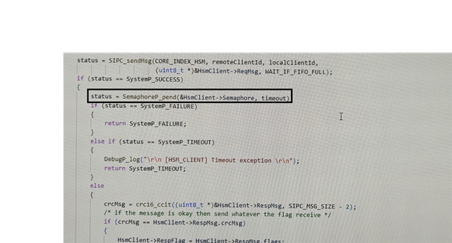
    I have successfully integrated the multi-core project with the Flash-based UART SBL. However, during image loading, the SBL gets stuck waiting for a semaphore release in the HSM’s SIPC while performing certificate verification. Could you please suggest how to resolve this issue?

    Regards,

    Shashank

  • Hi Shashank,

    Let me look into this and get back to you.

    Thanks and Regards,
    Aditya Singal

  • Hi Shashank,

    I'm closing this thread since it is unrelated to the last question and there is another thread for this question.

    Thanks and Regards,
    Aditya Singal