This thread has been locked.

If you have a related question, please click the "Ask a related question" button in the top right corner. The newly created question will be automatically linked to this question.

TMS320F28386D: Phantom powering of VDDA by VDDIO ?

Part Number: TMS320F28386D

Hello,

On our board we have separate power supplies for the 3.3V provided to VDDIO and VDDA.

The one on VDDIO is there some time before the other and we are seing the one on VDDA being phantom powered with a slow raise towards a diode voltage.

Could it come from there? Is there a clamping diode between VDDIO and VDDA inside the TMS320F28386D ?

Clément

  • Hi Clément,

    Your diagnosis is correct. The TMS320F28386D contains internal ESD protection diodes on every pin, and these are creating a current path from your powered VDDIO rail into the unpowered VDDA rail. The slow rise to approximately one diode drop below VDDIO is the textbook signature of this behavior [1].


    What's Happening Internally

    The device has ESD clamping diodes on its pins designed to limit voltages above VDDIO or below VSS [2]. When VDDIO is present but VDDA is not yet powered, these diodes become forward-biased and conduct current from VDDIO toward VDDA through the device's internal circuitry. The VDDA rail then charges slowly through this parasitic path — exactly the "phantom" ramp toward a diode voltage you're measuring [1].

    This is compounded by a key datasheet recommendation you are currently violating:

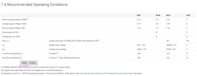
    It is strongly recommended that all 3.3V rails (VDDIO, VDDA, VDD3VFL, VDDOSC) be tied together and supplied from a single source. Supplying VDDA separately from VDDIO typically offers minimal benefits. [3]

    Additionally, the datasheet explicitly states that VDDIO, VDD3VFL, and VDDOSC must be maintained within 0.3V of each other during power-up [4]. Allowing VDDIO to rise significantly ahead of VDDA exceeds this tolerance and triggers the internal protection structures.


    Why This Is a Reliability Risk

    This isn't just a measurement curiosity — it's a potential damage scenario. The ESD clamping diodes have strict current limits [2]:

    Limit Type
    Maximum Current
    Continuous
    2 mA
    Peak
    20 mA

    If the current flowing from VDDIO to VDDA through these diodes exceeds these limits, the diode can fail catastrophically — resulting in a pin-level short to power or ground, or in severe cases, a power-to-ground short near that pin [2]. The datasheet also warns directly:

    If the recommended power sequence is violated, device malfunction and damage can occur as current will flow through unintended parasitic paths in the device. [3]


    Acceptable Power-Up Sequences

    The datasheet defines acceptable sequencing in Table 7-1 [5]. The key constraint is that VDDIO must power up first or simultaneously with VDDA — but critically, the rails are expected to track together, not have one lag significantly behind the other:

    Case
    Sequence
    A
    VDDIO → VDDA → VDD
    B
    VDDIO → VDD → VDDA
    G
    VDDIO + VDDA simultaneously → VDD

    None of the acceptable cases allow VDDA to power up before VDDIO, and none are designed to tolerate a large voltage gap between VDDIO and VDDA during the ramp [5].

    Also note: supply ramp rates faster than 10⁵ V/s on any of these rails can independently trigger the on-chip ESD protection [4], so ramp rate control matters as well.


    What You Should Do

    1. Preferred fix: Tie VDDIO and VDDA together to a single 3.3V supply as TI recommends [3]. Separate supplies on these rails provide negligible benefit and introduce exactly the sequencing risk you're experiencing.

    2. If separate supplies are required: Implement supply sequencing circuitry (e.g., a power sequencer IC or enable-pin control) to ensure VDDIO and VDDA ramp simultaneously and stay within 0.3V of each other throughout the power-up ramp [4].

    3. Verify current magnitude: Measure or estimate the current flowing into VDDA during phantom powering to confirm it stays below the 2mA continuous ESD diode limit [2]. If it exceeds this, your device may already be at risk of damage.


    A few things worth checking on your specific board:

    • How large is the capacitance on your VDDA rail? A larger cap will charge more slowly through the parasitic path and may make the phantom ramp more pronounced.
    • Are any analog pins (VREFHI, VDAC, etc.) being driven before VDDA reaches its operating voltage? The datasheet requires that no analog pin exceed VDDA + 0.3V before power-up [3], so a lagging VDDA could create a secondary violation on those pins as well.

    Citations

    1. TMS320F28386D – ESD Diode Behavior & Device Failure Discussion (E2E Forum)
    2. TMS320F28386D – VDD Above VDDIO Discussion (E2E Forum)
    3. TMS320F28386D Datasheet (SPRSP14E) – Page 102
    4. TMS320F28386D Datasheet (SPRSP14E) – Page 91
    5. TMS320F28386D Datasheet (SPRSP14E) – Page 104
    6. C2000 Technical Reference Manual (SPRUII0F) – Page 4029

    Best Regards,

    Zackary Fleenor

  • Hello,

    I am not sure to understand your first statement, do you confirm the phantom voltage comes from a path created by the ESD diodes internally to the device as VDDA is unpowered and VDD is ?

    Or from an external path ?

    I can't access the discussion from your first citation, it's either private or the link is incorrect.

    Note that you are refering to a recommendation we are violating, for sure, but a recommandation is something that is not enforced, otherwise it should be stated like that. And in none of the refered elements do I see that VDDIO and VDDA should be within 0.3V of each other (e.g.,  [5] does not say they have to be close from each other).

    Thank you,

    Clément

  • Any feedacks?

    Clément

  • Hey Clément,

    I apologize for the delayed response over the holiday weekend.

    Yes, the voltage comes from the path created by the ESD diodes internal to the device.

    Let me bring up the feedback regarding the associated wording with the internal team and determine what our best next steps would be here to improve this.

    Best Regards,

    Zackary Fleenor

  • Hi Zackary,

    Thanks for your feedback.

    So I do understand correctly that there are ESD diodes between the VDDIO and VDDA similarly to what's in one of the documents our FAE Anthony forwarded us this morning (SSYA010A) ?

    Which is not the case in that note btw. only the GND have diodes in-between.

    Clément

  • Hello Clément,

    I had a quick discussion with our team, we believe we need to make an update to the datasheet to include VDDA in the list below.

    Perhaps there may also be some confusion in my original wording here. The diodes creating these paths are not necessarily true "ESD" safety diodes as described in the SSYA0101A document, but rather, raw PN diode junctions hardcoded into the design of the power management system of the device.

    I hope this helps provide the necessary clarification and we will see what is needed to update the necessary wording/content.

    Best Regards,

    Zackary Fleenor

  • Hello Zackary,

    Understood, but then I would recommend you to put a "shall" or "must" as it's a mandatory condition not just an optional "should" condition.

    Could you please look at the following thread:
    https://e2e.ti.com/support/power-management-group/power-management/f/power-management-forum/1633052/tps62811-q1-tps628112a-q1-voltage-on-output-before-enable

    We have an issue with the 1.2V on one of the CPU too (but not both) so I am wondering if it could be some sort of diode as well between VDDIO and VDD?

    Best regards,

    Clément

  • Hey Clément,

    Agreed, we will determine the exact wording and provide the update in the next release.

    Your theory is certainly possible, let's close this thread in the meantime and follow up on the other thread. If the need arises, please create a new thread in the C2000 forum for additional debug/feedback.

    Best Regards,

    Zackary Fleenor