This thread has been locked.

If you have a related question, please click the "Ask a related question" button in the top right corner. The newly created question will be automatically linked to this question.

TMS320F28377D: DAC output error of F28377

Part Number: TMS320F28377D

Hi team,

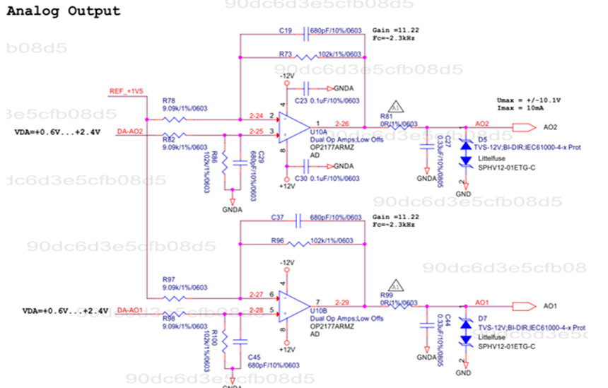
Our analog outputs are from U1 and T1 of the MCU (TI's TMS320F28377DZWTT). The DAC function outputs AO1 and AO2 after passing through the following circuit for customer use.

We completely replaced the following circuit for both issue models, but found the bias voltage still existed. Therefore, we traced back to the MCU and found that the MCU itself has a 0.02V drop at the command output. After amplification by 11.22 times, this becomes approximately a 0.2V voltage difference.

We would like to ask a few questions:

1. Does the MCU itself have an error in the DAC?

2. Does the error, caused by the VREFIA input power supply, also have an impact? Could you help confirm the relationship between the layers?

3. What are the specifications for the error section?
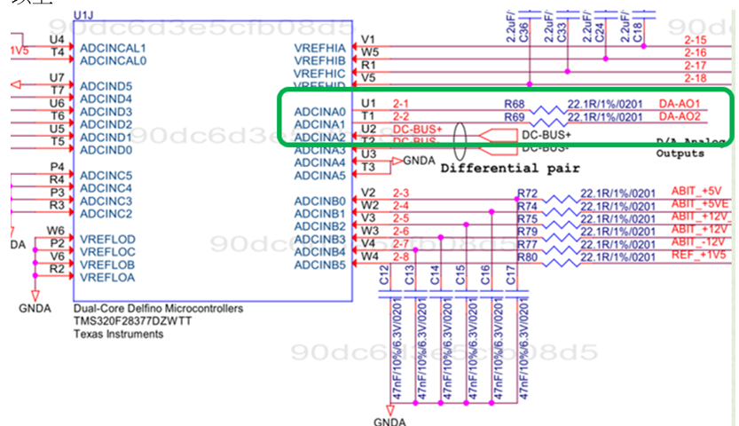
image.pngimage.png

  • Hello Jimmy,

    Before providing a complete answer, a few details would help refine the analysis:

    • What VREFHIA voltage are you using? (2.5V, 3.0V, or another value?) This matters because factory calibration is performed only at 2.5V.
    • Are you calling Device_cal() during initialization? This loads the factory offset trim values.
    • Do both AO1 and AO2 show the same 0.02V offset, or do they differ?

    That said, the retrieved specifications directly address your questions.


    Direct Answers

    1. Does the MCU DAC have inherent error?

    Yes. The 0.02V (20mV) offset you're measuring falls within the DAC's specified tolerance:

    Parameter Min Max Notes
    Offset Error -10 mV +10 mV At midpoint [1]
    Gain Error -2.5% +2.5% Of full-scale range [1]
    INL -5 LSB +5 LSB Endpoint corrected [1]

    Your 20mV observation is at the edge of the offset specification. After 11.22× amplification, this produces ~0.2V—which is expected behavior, not a defect.

    2. Does VREFHIA impact the error?

    Yes, directly. The DAC output follows this transfer function [2]:

    DACOUT = (DACVALA × DACREF) / 4096
    

    Any error, noise, or deviation in VREFHIA propagates proportionally to the output. Key requirements:

    • VREFHIA must be between 2.4V and VDDA [1]
    • If VREFHIA exceeds VDDA + 0.3V, an internal blocking circuit activates, causing improper output [1]
    • Proper decoupling is required: ≥1µF capacitor between VREFHIA and VREFLOA, placed close to the device [3]

    Critical: The DAC offset is factory-calibrated only at 2.5V reference [4]. If you're using a different VREFHIA voltage, you must manually adjust the offset trim using DAC_tuneOffsetTrim() to maintain datasheet performance [4].

    3. Error Specifications Summary

    Specification Value Citation
    Offset Error ±10 mV (at midpoint) [1]
    Gain Error ±2.5% FSR [1]
    INL ±5 LSB (typical ±2 LSB) [1]
    DNL ±1 LSB (typical ±0.4 LSB) [1]
    Linear Output Range 0.3V to VDDA − 0.3V [1]
    Reference Voltage Range 2.4V to VDDA [1]

    Recommended Actions

    1. Verify your VREFHIA voltage — If not 2.5V, use DAC_tuneOffsetTrim() to recalibrate [4]
    2. Check VREFHIA decoupling — Ensure ≥1µF capacitor is properly placed [3]
    3. Implement software compensation — Offset your DACVAL commands to account for the measured error at your specific operating point
    4. Confirm Device_cal() is called — This loads factory calibration values after reset [5]

    Conclusion

    Your 0.02V offset is within the DAC's specified error range and is expected behavior. The most likely path to eliminating the 0.2V post-amplification bias is either adjusting the offset trim (if using non-2.5V reference) or implementing software compensation in your DACVAL commands. If you can confirm your VREFHIA voltage and whether calibration functions are being called, I can provide more targeted guidance.


    References:

    1. TMS320F28377D Datasheet - DAC Electrical Specifications
    2. TMS320F28377D Technical Reference Manual - DAC Module
    3. TMS320F28377D Datasheet - Pin Configuration
    4. TMS320F28377D Technical Reference Manual - DAC Calibration
    5. TI E2E Forum - DAC Offset Trim Discussion

    Best Regards,

    Zackary Fleenor

  • Hi ,

    Thanks for your detailed explanation.

    • What VREFHIA voltage are you using? (2.5V, 3.0V, or another value?) This matters because factory calibration is performed only at 2.5V.
    • A: REF is 3V
    • Are you calling Device_cal() during initialization? This loads the factory offset trim values.
    • A: updear tracking 
    • Do both AO1 and AO2 show the same 0.02V offset, or do they differ?
    • A: only AO1 shows below. 
    •  
  • Hi Jimmy,

    I do not understand your second answer here. Can you provide further clarification?

    Best Regards,

    Zackary Fleenor

  • Hi Fleenor,

    Sorry, type wrong words. 

    • Are you calling Device_cal() during initialization? This loads the factory offset trim values.
    • A: customer no use the Device_cal() during initialization
  • Hi Jimmy,

    Thanks for confirming the customer is not calling `Device_cal()` during initialization. Given that, and the 3V VREFHIA voltage, the 0.02V offset is *expected* and significantly exacerbated.

    As we pointed out, the factory calibration is only performed at 2.5V. Without calling `Device_cal()`, the MCU is relying on potentially inaccurate default trim values when operating with a 3V reference. This effectively disables the initial offset compensation.

    Since only AO1 shows the offset, this could also indicate a slight channel-to-channel mismatch that’s becoming apparent with the lack of calibration, and the higher VREFHIA.

    **Here’s what we recommend the customer do, in order of priority:**

    1. **Implement `Device_cal()`:** This is the *most direct* solution. Adding this function call during initialization will load the factory trim values and likely bring the offset much closer to spec... potentially eliminating it altogether. They should re-test immediately after implementing this.

    2. **If `Device_cal()` isn't feasible (due to code constraints, etc.), implement `DAC_tuneOffsetTrim()`:** Since they are using 3V, they *must* manually calibrate the offset using `DAC_tuneOffsetTrim()`. This will require measuring the actual output offset on AO1 and adjusting the trim value accordingly. The Technical Reference Manual details the process.

    3. **Verify VREFHIA decoupling:** Just to confirm, is the ≥1µF capacitor between VREFHIA and VREFLOA present and physically close to the chip? Even though it's unlikely to *cause* a consistent 0.02V offset, it will contribute to noise and potentially stability issues.

    4. **Consider Software Compensation (as a last resort):** Only if the above steps don't yield satisfactory results should they resort to adjusting DACVAL commands in software to compensate for the offset. This is less ideal than proper calibration.

    Let us know if you have any further questions.

    Best Regards,

    Zackary Fleenor