This thread has been locked.

If you have a related question, please click the "Ask a related question" button in the top right corner. The newly created question will be automatically linked to this question.

TMS320F280039C: TMS320F280039C ADCC3 input pulled down during power event – Sample and Hold current question

Part Number: TMS320F280039C

Hello,

I am using TMS320F280039C and have a question about ADC Sample and Hold behavior on ADCC3.

PS_ON is an external switch signal and can be Low or Floating.
PS_ON is pulled up to 3.3 V through a 100 kohm resistor.
PS_ON_IN is used to sense PS_ON and is connected to ADC channel ADCC3 (ACQPS = 10).

Observed behavior is that when PS_ON is floating at 3.3 V and the main DCDC output (12V_main) turns off, PS_ON cannot maintain 3.3 V and temporarily drops close to 0 V, then rises again.
When PS_ON_IN is disconnected from the ADC pin (left open), PS_ON remains stable at 3.3 V.
This means the issue occurs only when ADCC3 is connected.
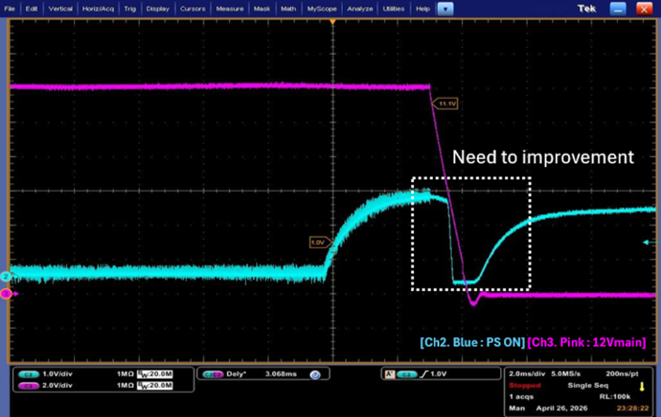
image.png

Based on the TRM input model for ADCC3, the total ADC input capacitance is about 11.3 pF and Ron is about 860 ohms.
With ACQPS = 10, the ADC Sample and Hold operation requires significantly more current than the 33 µA that can be supplied by a 100 kohm pull‑up.
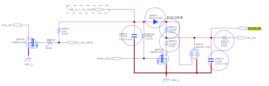
image.png

My questions are:

Is it possible that the ADCC3 Sample and Hold operation or internal analog structure can discharge an externally pulled‑up signal during a power event such as main output turn‑off?
With a high source impedance (100 kohm pull‑up), is ADC input voltage droop an expected behavior?
What source impedance or circuit topology does TI recommend when sensing a status signal like PS_ON using the ADC?

Thank you for your support.

  • Hello Jang,

    Thank you for the detailed question and excellent analysis. I can confirm that your observations are correct and the behavior you're seeing is directly related to the high source impedance combined with the ADC sample-and-hold operation.


    1. Can ADCC3 Sample and Hold discharge an externally pulled-up signal during a power event?

    Yes. The ADC sample-and-hold circuit contains an internal sampling capacitor (approximately 2.2 pF) plus additional parasitic capacitance (totaling approximately 11.3 pF as you calculated). During each sample phase, the internal switch closes and this capacitor must charge to the input voltage.

    With your 100 kohm pull-up resistor, the RC time constant is approximately 1.14 microseconds. Your 100 kohm resistor can only supply approximately 33 microamps (3.3V / 100kohm), but the sampling capacitor requires significantly more instantaneous current during the acquisition window. This creates a voltage droop on PS_ON that cannot recover quickly enough, particularly during power transients when the 12V_main rail is turning off.


    2. Is ADC input voltage droop expected with high source impedance (100 kohm)?

    Yes, this is expected behavior and outside the recommended operating conditions. According to the TMS320F280039C datasheet specifications:

    • Maximum recommended source impedance: 50 ohms or less
    • Minimum acquisition window: 75 ns (for 50 ohm source)

    Your 100 kohm source impedance is 2000 times higher than the recommended maximum. This will cause incomplete charging of the sampling capacitor, voltage droop during sample phases, potential ADC reading errors, and increased sensitivity to power transients.


    3. What source impedance or circuit topology does TI recommend?

    TI recommends the following solutions for high-impedance sources:

    Solution A: Add a Buffer Op-Amp (Recommended)

    Insert a unity-gain voltage follower between PS_ON and the ADC input:

    PS_ON (100kohm pull-up) → Op-Amp Buffer (low output impedance <10 ohms) → ADCC3

    The op-amp provides low output impedance to drive the ADC, isolates the high-impedance source from the ADC sampling current, and eliminates voltage droop during sampling and power transients.

    Op-Amp Selection Criteria:

    • Rail-to-rail input/output for 0-3.3V range
    • Low offset voltage (<1 mV)
    • Output impedance <10 ohms
    • Powered from a stable 3.3V rail (not 12V_main)

    Solution B: Increase Acquisition Window

    If you cannot add a buffer, significantly increase ACQPS to allow adequate settling time. For a 100 kohm source, you would need approximately 285 ACQPS cycles (assuming 50 MHz ADCCLK) to achieve 5-tau settling. However, this approach may still not fully resolve the power transient issue and significantly reduces ADC throughput.

    Solution C: Lower Source Impedance

    Reduce the pull-up resistor from 100 kohm to 1 kohm or lower. This increases current consumption from 33 microamps to approximately 3.3 milliamps but provides much better ADC performance and transient immunity.


    Recommended Circuit Modification:

    For your PS_ON sensing application, I recommend Solution A with the following topology:

    • Add a unity-gain buffer op-amp between the 100 kohm pull-up node and ADCC3
    • Add a 100 nF capacitor at the op-amp input for noise filtering
    • Ensure the op-amp is powered from a stable rail that remains active during 12V_main transients
    • Keep ACQPS = 10 (adequate with the low-impedance buffer output)

    This will completely eliminate the voltage droop you're observing and provide accurate ADC readings even during power events.

    Please let me know if you have any additional questions.

    Best Regards,

    Zackary Fleenor

  • Hello Zackary Fleenor

    Thank you for your detailed support
    We confirmed that adding a buffer resolves the issue correctly

    However, since the same PS_ON sensing structure was used in previous products without this issue, additional testing was performed to further understand the root cause

    The issue still occurs under all test conditions without hardware modification

    1. A 2.7 kohm pull-up was added to PS_ON, but the same behavior was observed. Lower resistance than 2.7 kohm cannot be used due to system constraints
    2. Disabling ADC on ADCC3 by removing ADC_setupSOC() did not resolve the issue
    3. Changing PS_ON_IN to a different ADC channel did not resolve the issue
    4. When the 12 V output is under no-load condition, PS_ON_IN remains stable and does not drop. When 12 V decreases slowly under no load, no issue is observed. However, if a load is suddenly applied during the no-load condition and 12 V drops rapidly, PS_ON_IN follows the same falling slope

    Based on these results, it seems there may be an additional discharge path inside the MCU beyond the sample and hold current effect

    Can you confirm whether any internal ADC input structure or power transient related mechanism could pull the input node down under this condition

    Thank you for your support

  • Hi Jang,

    Your follow-up testing conclusively demonstrates that this is not a sample-and-hold issue. The root cause is internal ESD protection diodes forward-biasing during the power transient, creating a discharge path that overwhelms your pull-up resistor regardless of ADC configuration.

    Here's what's happening: When 12V_main drops rapidly under load, the MCU's internal VDDA rail collapses. Once VDDA falls below approximately (V_PS_ON − 0.7V), the ESD protection diode between the ADC input pin and VDDA becomes forward-biased, sinking current from your PS_ON signal into the collapsing VDDA rail [1]. This diode current can reach several milliamps—far exceeding what even your 2.7 kΩ pull-up can supply (≈1.2 mA). This explains every observation:

    • Why disabling ADC didn't help: The ESD diodes are hardwired silicon structures that cannot be disabled via register configuration [1].
    • Why changing channels didn't help: All ADC input pins have the same ESD protection structure [1].
    • Why 2.7 kΩ still fails: The forward-biased diode sinks several mA, overwhelming a few-kΩ source [1].
    • Why it only occurs under load: A rapid 12V collapse causes VDDA to decay faster than the PS_ON signal, activating the diode. Under no-load, 12V decays slowly enough that VDDA tracks gracefully without creating the voltage differential needed to forward-bias the clamp [1].
    • Why previous products worked: Likely different power sequencing timing or load transient characteristics that kept VDDA from collapsing ahead of PS_ON.

    Two Additional Internal Mechanisms to Check

    1. OSDETECT Circuit: The Opens/Shorts Detection Circuit connects after the channel mux but before the S+H, providing an internal path to VSSA through 5 kΩ–7 kΩ resistors [2]. Verify your ADCOSDETECT register has DETECTCFG = 0 (Off). If inadvertently enabled, this creates a permanent discharge path to ground.

    2. CMPSS Mux Leakage: Over-voltages on other analog channels sharing the same CMPSS (Comparator Subsystem) multiplexer can create leakage currents that pull down adjacent channels—even with CMPSS disabled [3]. Check Table 6-8 in the datasheet to identify which channels share a mux with ADCC3, and ensure all unused analog inputs on that mux are tied to VSSA.


    Recommended Actions

    Priority
    Action
    Rationale
    1
    Keep the buffer op-amp (already validated)
    Isolates PS_ON from all internal discharge paths—ESD diodes, OSDETECT, and CMPSS leakage
    2
    Verify ADCOSDETECT register = 0
    Eliminates a potential 5–7 kΩ path to ground
    3
    Tie unused analog pins on the same CMPSS mux to VSSA
    Prevents cross-channel leakage during transients [3]
    4
    Ensure the buffer op-amp is powered from a rail that does not collapse with 12V_main
    If the op-amp supply also sags, the problem shifts to the op-amp output

    The buffer solution is correct and addresses the fundamental issue: your high-impedance PS_ON node cannot source enough current to overcome the MCU's internal protection structures during a power rail collapse event.


    For additional insight, it would be helpful to know:

    • Whether VDDA is derived from 12V_main or an independent source (this would confirm the ESD diode activation mechanism)
    • The timing relationship between 12V_main collapse and the 3.3V rail powering the pull-up resistor
    • Which other analog channels share the same CMPSS mux as ADCC3 (Table 6-8 in the datasheet)
    • Whether the MCU experiences a brown-out or remains fully powered during the 12V_main transient
    • The load current magnitude and slew rate on 12V_main that triggers the rapid voltage drop

    1. TMS320F280039C: ADC pin impedance when powered off - ESD diode behavior
    2. TMS320F28003x Technical Reference Manual - OSDETECT Circuit (Section 16.9)
    3. TMS320F280039C: ADC leakage current via CMPSS mux

    Best Regards,

    Zackary Fleenor

  • Hi Jang,

    I wanted to follow up on your PS_ON sensing issue to see if the buffer op-amp solution is still working well in your application, and whether you were able to investigate any of the additional internal mechanisms I mentioned.

    To recap, we confirmed the root cause was ESD protection diodes forward-biasing during the 12V_main power transient, creating a discharge path from PS_ON into the collapsing VDDA rail that overwhelmed your pull-up resistor.

    Quick checklist to further optimize your solution:

    1. Buffer op-amp installed (you've confirmed this works)
    2. ADCOSDETECT register verification – Can you confirm ADCOSDETECT.DETECTCFG = 0 to eliminate the potential 5–7 kΩ discharge path to ground?
    3. Unused analog pins – Have you tied any unused analog inputs sharing the same CMPSS mux as ADCC3 to VSSA? (See Table 6-8 in the datasheet)
    4. Op-amp power rail – Can you confirm the buffer op-amp is powered from a rail that remains stable when 12V_main collapses?

    If you have a moment, it would also be helpful to understand:

    • Is VDDA derived from 12V_main or an independent 3.3V source?
    • What is the timing relationship between the 12V_main collapse and your 3.3V pull-up rail?
    • Does the MCU experience a brown-out event during the 12V_main transient, or does it remain fully operational?

    This information would help me provide additional guidance on power sequencing or decoupling recommendations if needed, and may also help other customers facing similar transient immunity challenges.

    Please let me know if you have any remaining questions or if there's anything else I can assist with to close out this issue.

    Best Regards,

    Zackary Fleenor

  • Hello Zackary Fleenor
    Thank you for your detailed and helpful explanation.
    Based on your guidance, we performed additional verification and would like to confirm our understanding and ask a few follow-up questions.
    Additional verification results are as follows.

    1. After adding a buffer, the PS_ON signal no longer drops and remains stable during the power transient
    2. ADCOSDETECT is confirmed to be 0 (default value, not enabled)
    3. CMPSS mux unused pins are not floating, as they are connected to thermistor sensing ADC inputs
    4. Simultaneous measurements of VDD_S_3.3V_PSON, VDD_S_3.3VA, VREF, and VDDA show no observable voltage drop during the 12V transient event

    Based on these results, we would like to confirm the following points.
    First, since adding the buffer completely eliminates the PS_ON signal drop, we understand that the root cause is still consistent with ESD protection diode conduction during transient conditions. Can you confirm if this conclusion is correct?
    Second, we would like to clarify the VDDA behavior. Is the internal VDDA node inside the MCU identical to the external VDDA pin voltage, or is it possible for the internal VDDA node to momentarily collapse independently even if the external VDDA pin appears stable?
    Your clarification on these points would be greatly appreciated.
    Thank you for your support.
    Best regards
    Ki‑Young Jang

  • Hi Ki-Young,

    Thank you for the thorough follow-up testing. Your results are informative and actually require us to revise the root cause analysis from my previous response.


    Reassessment of Root Cause

    Your measurement result #4 is the critical finding. Because external VDDA remains stable during the transient, the voltage differential required to forward-bias the ESD clamp diode (V_PS_ON − V_VDDA > ~0.7V) never develops. ESD diode conduction was therefore likely not the primary root cause in your specific system.


    Revised Root Cause

    Most Probable Mechanism: Ground Bounce / VSSA Transient

    When 12V_main collapses rapidly under a sudden load step, large di/dt currents flow through the PCB ground plane. This creates a momentary VSSA bounce where the local analog ground reference inside the MCU rises transiently relative to the system ground at which your pull-up resistor is referenced.

    From the ADC input pin's perspective, the apparent input voltage becomes:

    V_apparent = V_PS_ON (referenced to system GND) minus V_VSSA (transiently elevated above system GND)

    The ADC input therefore appears to drop even though the PS_ON node is physically stable. This explains why VDDA appears stable on your scope -- you are measuring VDDA relative to the same reference that is bouncing, so the differential appears unchanged.

    Secondary Candidate: Capacitive Coupling via PCB

    The rapid dV/dt on the 12V_main plane during a hard load step can capacitively couple into adjacent signal traces. If the PS_ON_IN routing passes near the 12V_main plane or a switching node:

    I_coupled = C_parasitic x dV/dt

    As an example, with 0.5 pF parasitic capacitance and a dV/dt of 500 V/us, the coupled current is 250 uA. Against a 100 kohm pull-up this produces a 25V disturbance. Against a 2.7 kohm pull-up it is still 0.68V. Against a buffer output impedance below 10 ohms it becomes less than 2.5 mV and is negligible.

    Both mechanisms are fully consistent with all of your observations and both are resolved by the buffer, since its low output impedance can source or sink transient currents without allowing voltage droop at the ADC pin.


    Answers to Your Specific Questions

    Question 1: Is ESD diode conduction still the confirmed root cause?

    No. Based on your VDDA stability measurement, ESD diode forward-bias is not the primary mechanism in your system. The buffer solution remains correct and fully validated, but the root cause is more accurately described as VSSA ground bounce during the rapid 12V_main collapse, with capacitive coupling from the switching transient as a secondary contributor.

    Question 2: Can internal VDDA collapse independently of the external VDDA pin?

    This is a good question. The short answer is yes, it is theoretically possible but unlikely to be significant in your case.

    Between the external VDDA pin and the ADC core there is bond wire inductance on the order of 1 to 5 nH, internal ESD structures, and a limited internal decoupling capacitance on the order of 10 to 50 pF. Under fast transient conditions, L x di/dt voltage drops across the bond wire and internal IR drops could cause the internal VDDA seen by the ADC core to differ from the pin voltage by on the order of tens to perhaps 100 mV.

    However, even if internal VDDA dropped transiently by 200 mV, it would still only reach approximately 3.1V. Forward-biasing the ESD diode from a 3.3V PS_ON signal would require internal VDDA to fall below approximately 2.6V. The margin is too large for internal VDDA collapse to be the explanation in your case, and this mechanism does not account for your observations.


    Optional Additional Verification

    If you wish to confirm the root cause for documentation purposes, the following tests are suggested.

    To confirm ground bounce: measure the VSSA pin voltage relative to a remote ground reference point near the pull-up resistor during the 12V transient. A transient displacement of even 50 to 100 mV on VSSA would be sufficient to explain the observed behavior given your original 100 kohm source impedance.

    To confirm capacitive coupling: re-route the PS_ON_IN trace away from the 12V_main plane on a test board, or add ground guard traces on both sides of the signal. If the issue is reduced without the buffer, capacitive coupling is confirmed as a contributor.


    Summary

    The buffer op-amp solution is validated and resolves the issue regardless of which coupling mechanism is dominant. No further hardware changes are required. The previous ESD diode hypothesis is not supported by your VDDA stability measurement and should be considered ruled out. The root cause is consistent with VSSA ground bounce and capacitive coupling from the 12V_main transient event.

    Please let me know if you have any remaining questions or would like help interpreting measurements from the optional verification tests.

    Best Regards,

    Zackary Fleenor

  • Hello Zackary Fleenor

    Thank you for your detailed explanation and updated root cause analysis.
    Based on your suggestions, we performed additional verification and would like to share the results and ask for further clarification.

    First, regarding capacitive coupling from the 12V_main transient, we performed an additional test by rerouting the PS_ON signal using a wire jumper to minimize PCB coupling effects. However, the same PS_ON_IN voltage drop was still observed, indicating that capacitive coupling is unlikely to be the dominant contributor in our system.

    Second, regarding the ground bounce/VSSA transient explanation, we compared this behavior with a previous product that uses a similar circuit configuration. In the previous design, no PS_ON signal drop was observed under the same conditions.
    Upon reviewing the PCB layout, we found a key difference in the MCU grounding structure.
    In the previous product, the MCU grounds (VSS and VSSA) are separated, whereas in the current design, VSS and VSSA are directly connected without isolation.

    Based on this difference, we would like to ask the following questions:
    1. Is it possible that the connection (or separation) of MCU digital ground (VSS) and analog ground (VSSA) significantly affects ground bounce or VSSA transient behavior under high di/dt conditions?
    2. Do you have any recommended guidelines for grounding (specifically VSS and VSSA separation or connection) for the TMS320F280039C, especially in systems with fast power transients such as our 12V_main load step condition?
    3. Any guidance on grounding best practices or layout recommendations would be greatly appreciated.

    Thank you for your support.
    Best regards
    Ki‑Young Jang

  • Hi,

    The expert is currently out of office. Please expect a delay in response until they return next week. 

    Kind regards,
    AJ Favela 

  • Hi Ki-Young,

    Excellent investigative work. Your wire jumper test and comparison with the previous product design have provided the critical clue. The difference in VSS/VSSA grounding architecture is highly likely to be the root cause of the behavior difference between your current and previous products.


    Question 1: Does VSS/VSSA connection vs. separation significantly affect ground bounce behavior?

    Yes, absolutely. This is one of the most common causes of ADC performance issues in mixed-signal MCU designs, particularly under high di/dt transient conditions.

    When 12V_main collapses rapidly under load, large transient currents flow through the PCB ground plane, creating voltage drops according to V_drop = I_transient × Z_ground.

    Current Design (VSS and VSSA Connected):

    When VSS and VSSA are directly connected without isolation, the digital return currents from the MCU core, peripherals, and external switching loads share the same ground path as the sensitive analog reference. The transient current creates a voltage disturbance that appears directly on VSSA. The ADC measures voltages relative to VSSA. When VSSA rises transiently by 100 mV due to ground bounce, a 3.3V input signal appears to the ADC as 3.2V, creating the voltage drop you observe on PS_ON_IN.

    Previous Design (VSS and VSSA Separated):

    When VSS and VSSA are separated and connected only at a single star-point near the power supply, the digital return currents flow through the VSS path while the analog reference remains isolated on the VSSA path. The transient current disturbance is confined to VSS and does not couple into VSSA. This explains why your previous product did not exhibit the PS_ON signal drop under identical conditions.


    Questions 2 & 3: Recommended VSS/VSSA Grounding Guidelines for TMS320F280039C

    TI provides specific grounding recommendations in the TMS320F280039C datasheet (Section 9.2.5) and the TMS320F28003x Technical Reference Manual (Section 5.3). Here are the key best practices:

    A) VSS and VSSA Star-Point Connection (Recommended)

    VSS and VSSA should be connected at a single star-point located as close as possible to the power supply entry point or bulk decoupling capacitors. All VSS pins should connect to a dedicated digital ground plane. All VSSA pins should connect to a dedicated analog ground plane. The two planes should be separated throughout the PCB and joined only at the star-point.

    Benefits:

    • Isolates digital switching noise from analog ground reference
    • Prevents high di/dt digital currents from creating voltage drops on VSSA
    • Maintains clean analog reference for ADC, DAC, and comparator subsystems

    Implementation:

    • The star-point should be located near the voltage regulator output or main power entry
    • Use low-inductance, wide copper connections from all ground pins to their respective planes
    • Place bulk decoupling capacitors (10 µF, 1 µF) at the star-point
    • Ensure the star-point connection has very low impedance

    B) Split Ground Plane Strategy

    Create a dedicated analog ground island under the MCU analog section (ADC pins, VDDA, VREFHI/LO, VSSA) and a separate digital ground plane for the rest of the MCU and system. Connect the analog island to the digital plane only at the star-point.

    Critical routing guidelines:

    • Route all analog signals over the analog ground island
    • Avoid routing digital signals over the analog ground island
    • PS_ON_IN and other ADC input signals should route exclusively over the analog ground island
    • Keep ADC input traces short and direct
    • Do not allow high-current digital return paths from 12V_main load to flow under or near the analog ground island

    C) Decoupling Capacitor Placement

    For VDDA:

    • Place 1 µF ceramic capacitor within 5 mm of each VDDA pin
    • Place 10 µF ceramic or tantalum bulk capacitor within 10 mm
    • Connect capacitors directly to the analog ground island (VSSA)
    • Use low-inductance connections (short, wide traces or multiple vias)

    For VDD:

    • Place 0.1 µF ceramic capacitor within 5 mm of each VDD pin
    • Place 1 µF and 10 µF bulk capacitors within 10 mm
    • Connect capacitors to the digital ground plane (VSS)

    D) VSSA Pin Connection

    The TMS320F280039C has multiple VSSA pins. All VSSA pins must be connected to the analog ground island with low impedance:

    • Use multiple vias (via stitching) from each VSSA pin to the analog ground plane
    • Do not leave any VSSA pin floating or weakly connected
    • Minimize trace length from VSSA pins to the ground plane


    Specific Recommendations for Your Design

    Immediate Actions (current design with VSS/VSSA connected):

    1. Keep the buffer op-amp - This remains the correct solution and provides isolation from ground bounce effects regardless of the grounding architecture

    2. Verify decoupling capacitors - Ensure 1 µF capacitors are placed within 5 mm of each VDDA pin, connected to VSSA with low impedance

    3. Add ferrite bead isolation (optional) - If redesign is not possible, consider inserting a ferrite bead between the VSS/VSSA connection point to provide high-frequency isolation while maintaining DC continuity. Use a bead with DC resistance less than 100 milliohms, impedance at 10 MHz of 100-300 ohms, and rated current greater than maximum MCU current draw.

    Long-Term Design Improvements (next PCB revision):

    1. Implement star-point grounding - Separate VSS and VSSA planes, connect only at power supply entry point

    2. Create analog ground island - Dedicate a ground region under the MCU analog section, connected to main ground only at star-point

    3. Reroute PS_ON_IN - Ensure trace routes exclusively over analog ground island, away from 12V_main switching currents

    4. Add ground stitching - Use via arrays to create low-impedance connections from VSSA pins to analog ground plane

    5. Review 12V_main load return path - Ensure high di/dt return currents from the 12V load do not flow through or near the analog ground region


    Why Your Previous Product Worked

    Your previous product's separated VSS/VSSA architecture provided natural isolation. Digital switching currents (including 12V_main load transients) flowed through the VSS path while VSSA remained stable and unaffected by the transient. The 100 kohm pull-up was sufficient because there was no ground bounce on VSSA to create an apparent voltage drop. No buffer was needed because the ADC input voltage remained stable relative to VSSA.

    In your current design, the connected VSS/VSSA allows ground bounce to couple directly into the analog reference, overwhelming the high-impedance source.


    Additional Verification Test

    To conclusively confirm ground bounce as the root cause, perform this measurement:

    Test Setup:

    • Use a differential probe or two-channel oscilloscope
    • Channel 1: Measure PS_ON_IN (ADC input) referenced to VSSA pin on MCU
    • Channel 2: Measure VSSA pin referenced to a remote ground point (at the power supply or pull-up resistor ground)
    • Trigger on the 12V_main collapse event

    Expected Results if Ground Bounce is the Cause:

    • Channel 1 (PS_ON_IN relative to VSSA): Should remain stable at 3.3V
    • Channel 2 (VSSA relative to remote ground): Should show a transient spike during the 12V collapse

    This would directly demonstrate that PS_ON_IN is stable relative to the local VSSA, but VSSA itself is bouncing relative to the system ground reference.


    Reference Documents

    For additional details, please refer to:

    1. TMS320F280039C Datasheet (SPRSP61) - Section 9.2.5: Power Supply Decoupling and Layout Guidelines, Section 9.3: PCB Layout Recommendations

    2. TMS320F28003x Technical Reference Manual (SPRUIX1) - Section 5.3: System Design Guidelines, Section 16.3: ADC Electrical Characteristics and Operating Conditions

    3. TI Application Report: "PCB Layout Guidelines for Mixed-Signal Systems" (SLYT499)

    4. TI Application Report: "Grounding in Mixed-Signal Systems Demystified" (SLYT512)


    Summary

    Root Cause: Ground bounce on VSSA due to shared VSS/VSSA connection allowing digital transient currents to create voltage disturbances on the analog reference.

    Why Previous Product Worked: Separated VSS/VSSA architecture isolated analog ground from digital switching noise.

    Current Solution: Buffer op-amp remains the correct and validated solution. It provides low output impedance that can source/sink transient currents without voltage droop, effectively isolating the ADC input from ground bounce effects.

    Long-Term Recommendation: Implement star-point grounding with separated VSS/VSSA planes in next PCB revision for optimal mixed-signal performance.

    Please let me know if you need clarification on any of these recommendations or if you would like assistance with the differential ground measurement test to conclusively confirm the ground bounce mechanism.

    Best Regards,

    Zackary Fleenor