Part Number: TMS320F28P650DK
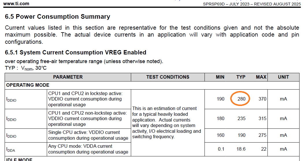
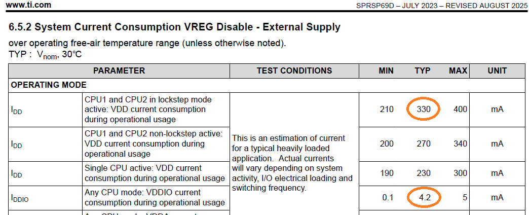
I'm having trouble making sense of the "VREG Enabled" vs "VREG Disable - External Supply" specs in the datasheet (SPRSP69D – JULY 2023 – REVISED AUGUST 2025).
If I understand the internal power architecture correctly, VDDIO (3.3V) feeds the internal VREG which, when enabled, can supply the VDD (1.2V). Also, I understand that the internal VREG is a linear regulator.
It seems that when VREG is enabled that IDDIO (measured externally) should be the sum of the internal IDDIO (for the IO and other uses) + IDD (from VREG, to the core).
When VREG is disabled and an external VDD is used, IDDIO + IDD should be roughly the same at the total IDDIO when VREG is enabled.
I do understand that the total power into the chip drops when VREG is disabled and an external regulator used, which makes sense.
I don't understand why it seems that the 1.2V supply's current seems to increase when using an external VDD regulator -- it's counterintuitive.
Could you explain why this spec is written this way? Examples from the two areas of the datasheet are below.