


Part Number: TMS320F2800137
Other Parts Discussed in Thread: MSPM0C1105
Hi Expert,
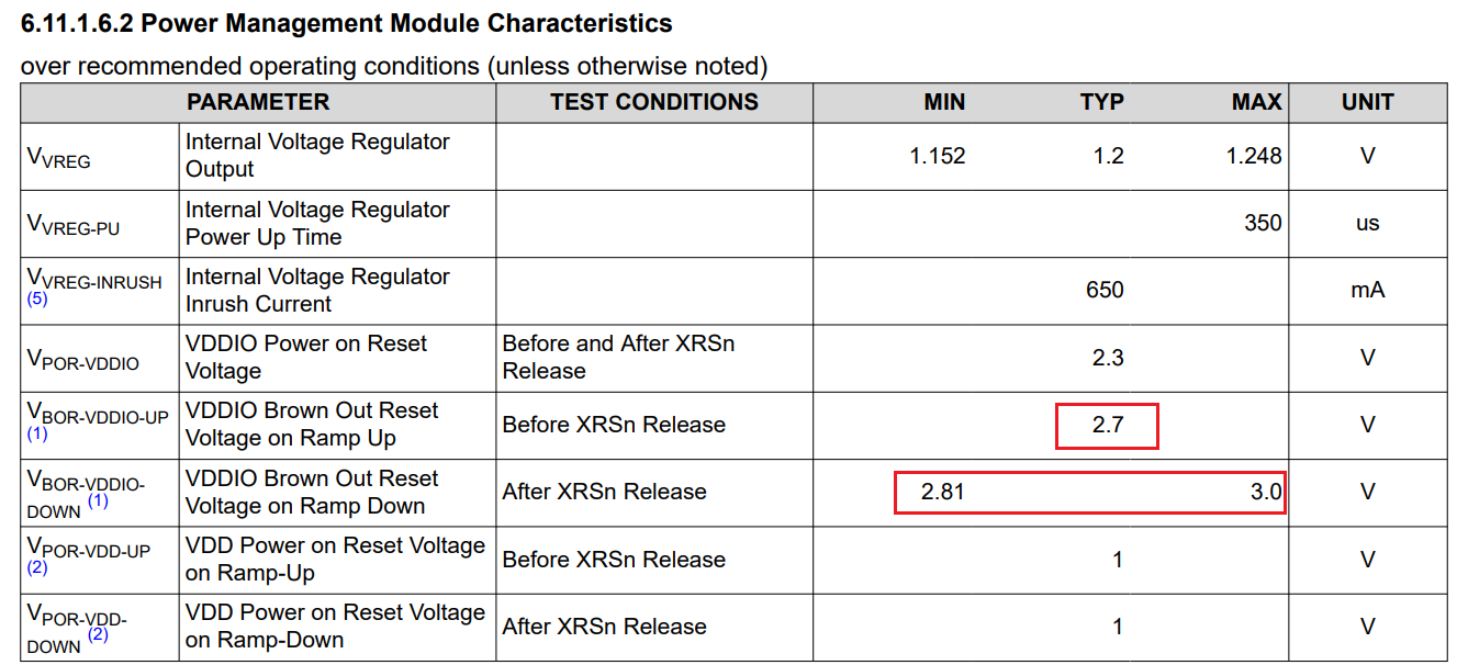
In VDDIO-BOR circuit, we can see it covers two threshould: BOR-VDDIO-UP and BOR-VDDIO-DOWN, from my understanding it is used in power up and power down seperately, that means:
- During power up, when VDDIO voltage meet BOR-VDDIO-UP value, the device will release XRSn and start to work.
- During power down, when VDDIO voltage meet BOR-VDDIO-DOWN value, the device will hold XRSn with Low.
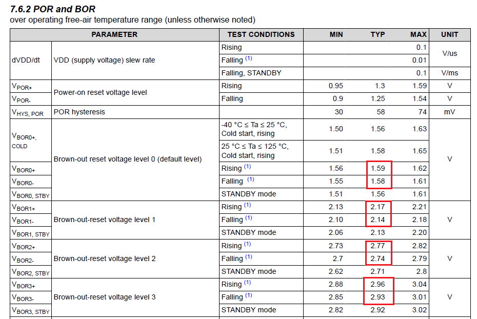
From my understand, BOR-VDDIO-UP should be larger than BOR-VDDIO-DOWN, to avoid un-wanted level jumping. In TI other MCU like MSPM0C1105, BOR-UP also higher than BOR-DOWN:
However in F2800137 datasheet, BOR-UP is 2.7V while BOR-DOWN is 2.81V min and 3.0V max, if user application VDDIO is fix 2.9V, that would make the chip trig the BOR-UP and BOR-DOWN continuously, that seems not acceptable for end customer, what's the key purpose of this design? Could you explain more detail of this BOR mechanism? Thanks.
Wiky
