This thread has been locked.

If you have a related question, please click the "Ask a related question" button in the top right corner. The newly created question will be automatically linked to this question.

TMS320F28P550SJ: How to enable all ADC Analog Groups on TMS320F28P550SJ9?

Part Number: TMS320F28P550SJ
Other Parts Discussed in Thread: LAUNCHXL-F28P55X, C2000WARE

Hi TI Team,

I am using the TMS320F28P550SJ9 EVM and have observed that ADC channels belonging to one analog group are working correctly, while channels from other analog groups do not appear to respond as expected.

For example:

  • ADCA0 channel is working.
  • ADCB5 is working.
  • ADCB0 and ADCB2 are not providing expected conversion results.

I reviewed the TRM, datasheet analog-group tables, and asysctl.h, but I could not find any API or register setting that explicitly enables/disables Analog Group 1 or Analog Group 2.

Questions:

  1. Is there any software configuration required to enable Analog Group 1 and Analog Group 2 ADC channels?
  2. Are analog groups always enabled by default after ADC initialization?
  3. Are there any Analog Subsystem (ASysCtl) registers that must be configured before channels from all analog groups can be sampled?
  4. Could EVM routing or package limitations cause only a subset of ADCB channels to be accessible?
  • Hi Anusha,

    Can you help me with the following questions to understand this better.

    1. When you say channel is working and not working what do you mean? Did you apply a certain voltage externally and monitor the ADC conversion result? Please note that if you leave the pin floating, the converted value will be non-deterministic.

    2. Have you followed the steps provided in C2000 examples to test the ADC configuration?

    3. A0 and B5 are from different groups. Since both are working to rule out the possibility of different groups can you try other channels to see if it is working. 

    Reagrds,
    Harisyam

  • Hi Harisyam,

    Thank you for your response.

    1. By "working" and "not working", I mean that I applied an external 3.3 V DC input to the ADC channel under test and monitored the ADC conversion result.

      • Channels that are working produce ADC counts close to the expected full-scale value for a 12-bit ADC.
      • Channels that are not working do not produce the expected ADC counts when the same 3.3 V input is applied.

      The channels are not left floating during testing.

    2. Yes, I have followed the ADC configuration flow from the C2000 examples. The ADC modules are enabled, SOCs are configured, and conversions are triggered through ePWM.

    3. Based on my testing:

      Working channels:

      • ADCA channels belonging to Analog Group A are working properly.
      • ADCB5, ADCB7, and ADCB9 are working correctly.

      Channels not producing the expected ADC result with an applied 3.3 V input:

      • ADCB0
      • ADCB1
      • ADCB2
      • ADCB4
      • ADCA2
      • ADCA9
      • ADCA10
      • ADCC1
      • ADCC8
      • ADCC10
      • ADCC11

      I also noticed that several of the above channels are associated with the analog-group multiplexing shown in the device documentation.

    Since some channels from ADCA, ADCB, and ADCC are working correctly while others are not, I would like to understand:

    • Is there any additional Analog Subsystem (ASysCtl) configuration required for channels belonging to Analog Groups 2, 3, and 4?
    • Are all analog groups enabled by default after ADC initialization?
    • Are there any package-specific or EVM-specific routing limitations affecting ADCINB0, ADCINB1, ADCINB2, ADCINB4, ADCINA2, ADCINA9, ADCINA10, ADCINC1, ADCINC8, ADCINC10, and ADCINC11?
    • Are any of these channels shared with CMPSS/PGA input muxing in a way that requires additional configuration before ADC conversions can be performed?

    Any guidance on how to verify whether the issue is related to analog-group routing, package availability, EVM connections, or additional analog subsystem configuration would be greatly appreciated.

    Thank you

  • Hi Anusha,

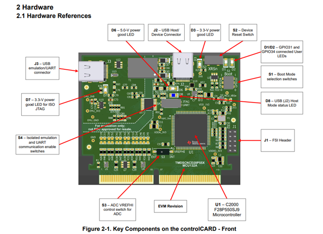
    Are you using the control card? Can you also verify if you have correctly put the ADC VREFHI control switch.

    Additional configurations are not required if you have few channels working. I will check again.

    Regards,
    Harisyam

  • Hi Harisyam,

    I am using the TI LaunchPad evaluation board based on the TMS320F28P55x microcontroller (F28P550SJ9).

    Since ADCB5, ADCB7, and ADCB9 are producing the expected ADC conversion results when a 3.3 V external input is applied, I believe the ADC reference is functioning correctly.

    Could you please clarify the recommended S3 (ADC VREFHI control switch) position for ADC testing on the TMS320F28P55x LaunchPad/Evaluation Board so that I can verify it matches the expected configuration?

    For reference, during ADC testing with a stable external 3.3 V input:

    Working channels:

    • ADCB5
    • ADCB7
    • ADCB9

    Channels not producing the expected ADC result:

    • ADCB0
    • ADCB1
    • ADCB2
    • ADCB4
    • ADCA2
    • ADCA9
    • ADCA10
    • ADCC1
    • ADCC8
    • ADCC10
    • ADCC11

    Since several channels across multiple ADC modules are functioning correctly, I would like to understand whether there are any LaunchPad/EVM-specific routing, channel availability, jumper, switch, or VREF-related considerations that could affect these particular ADC inputs.

    Thank you.

  • Hi Anusha,

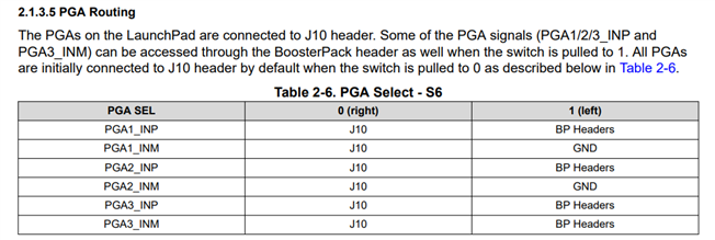
    There is a switch S6 in launchpad which makes the connection of microcontroller pin to J10 or the regular booster pack. Can you check if this is connected in the right location.

    The configuration for this is available in launchpad schematic.

    Regards,
    Harisyam

  • Hi Harisyam,

    I checked the S6 (PGA Select Switch) configuration on my LaunchXL-F28P55X evaluation board. The switch was already in the DOWN position, which routes the PGA signals to the J10 headers according to the LaunchPad schematic.

    Even with S6 in this position, I am still observing the same behavior.

    When applying a stable external 3.3 V input and monitoring the ADC conversion results:

    Channels producing expected ADC results:

    • Module A: A0, A1, A3, A4, A5, A12
    • Module B: B5, B7, B8, B9, B15
    • Module C: C0, C3, C5, C15

    Channels not producing the expected ADC results:

    • Module A: A2, A9, A10
    • Module B: B0, B1, B2, B4, B6
    • Module C: C1, C8, C10, C11

    Since the S6 switch is already configured for the J10 header path and multiple channels across ADCA, ADCB, and ADCC are functioning correctly, it appears that the ADC modules and reference configuration are working.

    Could you please advise whether these specific channels have any additional LaunchPad routing, jumper settings, package limitations, analog mux dependencies, or board-level connections that should be verified?

    Thank you.

  • Hi Anusha,

    S6 (PGA Select Switch) launchpad needs to be in up position to make the connections to the booster pack. 

    C:\ti\c2000\C2000Ware_26_01_00_00\driverlib\f28p55x\examples\adc\adc_ex10_multiple_soc_epwm example code in C2000Ware was tested in launchpad with S^ pin in up position to sample A2 pin and the right results were observed. 

    Can you try this example with the S6 switch in up position?

    Regards,
    Harisyam

  • Hi Harisyam, 

    After moving S6 to the UP position, the PGA positive input channels (PGAx_P) are now producing the expected ADC conversion results.

    However, I noticed that the corresponding PGA negative input channels do not appear to behave the same way.

    Specifically:

    • PGA1_N (A3)
    • PGA2_N (B12)
    • PGA3_N (B11)

    appear to be grounded or do not respond to an externally applied test voltage in the same manner as the PGAx_P channels.

    Could you please clarify whether this behavior is expected on the LaunchXL-F28P55X board?

    Are these PGAx_N signals tied to ground, terminated, or routed differently on the LaunchPad hardware?

    Also, from a system design perspective, if we design a custom PCB using the same TMS320F28P55x device, will these PGA negative input channels be fully available for user routing and ADC measurement, or is there any device-level limitation associated with these inputs?

     is this a LaunchPad-specific routing implementation, or should the same behavior be expected on a custom board as well?

    Thanks.

  • Hi Anusha,

    This is launchpad specific connection as discussed in section 2.1.3.5 PGA routing of EVM user guide. 

    For more details, please refer the following document

    EVM schematic: LAUNCHXL-F28P55X Schematic (Rev. A) 

    EVM user guide: https://www.ti.com/lit/ug/sprujc0a/sprujc0a.pdf?ts=1783320533322&ref_url=https%253A%252F%252Fwww.ti.com%252Ftool%252FLAUNCHXL-F28P55X 

    Regards,
    Harisyam