TMS320F280039C: GPyDAT and GPyDAT_R description and figure discrepancy

Part Number: TMS320F280039C

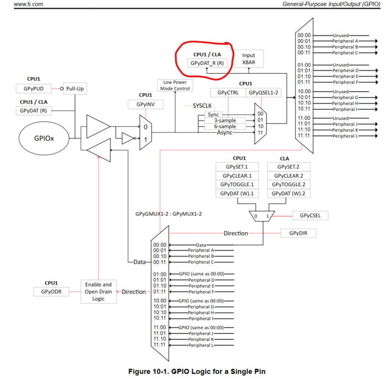
TI's literature SPRUIW9C (TMS320F28003x TRM) section 10.5 has contradictory statements regarding GPyDAT and GPyDAT_R which don't agree with Figure 10-1 (please see attached screenshots).  Figure 10-1 shows "GPyDAT_R (read)" label at the post-qualification tap, which conflicts with the text in section 10.5, which says that GPyDAT shows the current state of the GPIO pin after qualification.

Following statements are contradictory in the cited sections:

“10.5 Digital General-Purpose I/O Control

• GPyDAT Registers

No matter how the pin is configured (GPIO or peripheral function), the corresponding bit in the data register reflects the current state of the pin after qualification. Writing to the GPyDAT register clears or sets the corresponding output latch and if the pin is enabled as a general-purpose output (GPIO output), the pin is also driven either low or high. If the pin is not configured as a GPIO output, then the value is latched but the pin is not driven. Only if the pin is later configured as a GPIO output is the latched value driven onto the pin.

The GPyDAT registers reflect the state of the pin, not the latch. This means the register reflects the actual pin value. 

• GPyDAT_R Registers

The GPyDAT_R registers are read only registers that return the value written to the GPyDAT registers instead of pin status. Writes to these registers have no effect."

(1)  The above text and placement of GPyDAT_R register in figure 10-5 don't agree.

(2)  The description under 10.5 (GPyDAT) says "No matter how the pin is configured (GPIO or peripheral function), the corresponding bit in the data register reflects the current state of the pin after qualification".  But then, another statement under the same heading says "If the pin is not configured as a GPIO output, then the value is latched but the pin is not driven. ".

Above statement means that if pin is not configured as a GPIO, then, writing to GPyDAT latches that value in that register, but doesn't drive that value to the pin.  Then, certainly, that GPyDAT register bit cannot reflect the state of the pin after qualification, which is contradictory to the first statement.


Kindly clarify which explanation is correct (or provide the correct explanation).  Please also clarify if the figure is incorrect.  If incorrect, is there a corrected figure available?

Regards.

Nitish
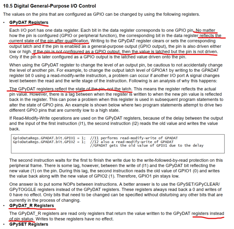
 

image.png

image.png

  • Hi,

    The key distinction is that reading and writing GPyDAT access different hardware paths.

    Read GPyDAT: Returns the GPIO pin status, rather than the output-latch value.
    Write GPyDAT: Updates the GPIO output latch. This value drives the pin only when it is configured as a GPIO output.
    Read GPyDAT_R: Returns the stored output-latch value, rather than the GPIO pin status.
    Write GPyDAT_R: Has no effect.

    GPyDAT_R provides readback of the written value and should not be used to read external inputs. 

    Regarding item (2), the statements about GPyDAT are not contradictory. Writing a value updates the output latch; it does not change the source used when reading GPyDAT. For example, if a pin is configured as an input and externally held low, writing a 1 to its GPyDAT bit stores a 1 in the output latch without driving the pin. Reading GPyDAT still returns 0, while reading GPyDAT_R returns the stored 1.

    I see the inconsistency in figure and I'll report this to be fixed on next release.

    Best regards,

    Masoud

  • Hello Masoud,

    Thank you for your response.  In your example case when a pin is configured as an input and externally held low, I am trying to understand why reading GPyDAT returns 0 even when a 1 has been written to GPyDAT bit and its output is latched to 1.

    I think you are saying that the source is the GPIO pin.  Is that correct?

    Would you mind explaining how that source is connected to the GPyDAT register so that when GPyDAT is read, it returns the state of the source?

    Is there a diagram showing how the source is connected to the GPyDAT flip-flop to allow it to return the state of the source instead of the state of its latched output?

    I used to think that a GPyDAT register bit only would contain the value that is latched in it, so reading that bit should return that same value.  This is untrue based on your explanation.

    Thank you, in advance.

    Nitish

  • To clarify the general behavior:

    GPyDAT (Write): This register interacts with the output latch. When you write to it (or use the SET/CLEAR/TOGGLE registers), you are updating the value that will be driven onto the pin if the pin is configured as a GPIO output.

    GPyDAT_R (Read): This is intended as an internal read-back register that returns the value currently held in the output latch, rather than the physical state of the pin.

    The confusion in the text often arises because the "read" path for the physical pin state is separate from the "read" path for the output latch. If you are looking to read the actual physical state of the pin (after qualification), you typically monitor the input path, whereas GPyDAT_R is specifically designed for software to verify what was previously written to the output register without needing to read the physical pin voltage.

    Best,

    Masoud

  • Hello Masoud,

    Thank you for your response.  Is it correct to understand then, that writing to the same corresponding bit "n" of any of the four registers in a block (say, bit 2 of GPBDAT, GPBSET, GPBCLEAR and GPBTOGGLE) acts on the same single latch?  Meaning, each of the corresponding register bits don't have their own latches but control a single latch?

    Regards,

    Nitish

  • Hi,

    Yes, your understanding is correct. Each GPIO has one output latch, and the corresponding bits in GPBDAT, GPBSET, GPBCLEAR, and GPBTOGGLE provide different ways to update that same latch.

    For your example, bit 2 corresponds to GPIO34:

    Register

    Effect on GPIO34’s output latch

    GPBDAT, bit 2

    Writing 0 clears it; writing 1 sets it.

    GPBSET, bit 2

    Writing 1 sets it.

    GPBCLEAR, bit 2

    Writing 1 clears it.

    GPBTOGGLE, bit 2

    Writing 1 inverts it.

    Writing 0 to GPBSET, GPBCLEAR, or GPBTOGGLE has no effect. These are operation registers; they do not maintain separate output values. 

    GPBDAT_R, bit 2, reads back this same output latch, whereas GPBDAT, bit 2, reads the pin status. The latch drives the pin only when it is configured as a GPIO output. 

    Best regards,

    Masoud